

Top-down digital design flow - Microelectronic Systems Laboratory
Top-down digital design flow - Microelectronic Systems Laboratory
Top-down digital design flow - Microelectronic Systems Laboratory

You also want an ePaper? Increase the reach of your titles
YUMPU automatically turns print PDFs into web optimized ePapers that Google loves.
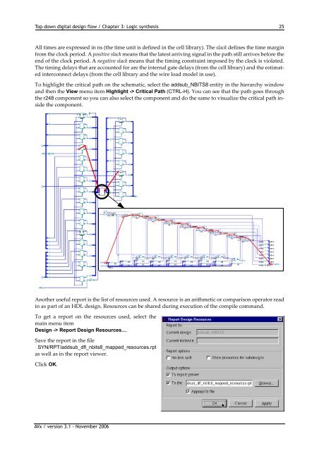
<strong>Top</strong>-<strong>down</strong> <strong>digital</strong> <strong>design</strong> <strong>flow</strong> / Chapter 3: Logic synthesis 25All times are expressed in ns (the time unit is defined in the cell library). The slack defines the time marginfrom the clock period. A positive slack means that the latest arriving signal in the path still arrives before theend of the clock period. A negative slack means that the timing constraint imposed by the clock is violated.The timing delays that are accounted for are the internal gate delays (from the cell library) and the estimatedinterconnect delays (from the cell library and the wire load model in use).To highlight the critical path on the schematic, select the addsub_NBITS8 entity in the hierarchy windowand then the View menu item Highlight -> Critical Path (CTRL-H). You can see that the path goes throughthe r248 component so you can also select the component and do the same to visualize the critical path insidethe component.Another useful report is the list of resources used. A resource is an arithmetic or comparison operator readin as part of an HDL <strong>design</strong>. Resources can be shared during execution of the compile command.To get a report on the resources used, select themain menu itemDesign -> Report Design Resources....Save the report in the fileSYN/RPT/addsub_dfl_nbits8_mapped_resources.rptas well as in the report viewer.Click OK.AVx / version 3.1 - November 2006


