

Top-down digital design flow - Microelectronic Systems Laboratory
Top-down digital design flow - Microelectronic Systems Laboratory
Top-down digital design flow - Microelectronic Systems Laboratory

Create successful ePaper yourself
Turn your PDF publications into a flip-book with our unique Google optimized e-Paper software.
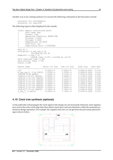
<strong>Top</strong>-<strong>down</strong> <strong>digital</strong> <strong>design</strong> <strong>flow</strong> / Chapter 4: Standard cell placement and routing 44Another way to do a timing analysis is to execute the following commands in the Encounter console:encounter 15> setCteReportencounter 16> reportTAThe following report is then displayed in the console:*info: Report constrained paths* Path type: max* Format: long* Operating Condition: WORST-IND* Process: 1.4000* Voltage: 3.0000* Temperature: 85.0000* Time Unit: 1ns* Capacitance Unit: 1.000000pf----------------------------------------------------------------------------Path #: 1Startpoint: b_reg_reg_0_/Q(clocked by clk R)Endpoint: z_reg_7_/D(Setup time: 0.007, clocked by clk R)Data required time: 9.993Data arrival Time: 7.705Slack: 2.288Object name Delta r/f (ns) Sum r/f (ns) Slew (ns) Load (pf)----------------------------------------------------------------------------clk 0.000r/-f 0.000r/-f 0.000r/0.000f 0.174b_reg_reg_0_ C->Q (DFC3) 1.078f/-r 1.078f/-r 0.000f/0.000r 0.016r248/U9 B->Q (XNR20 1.059f/-r 2.137f/-r 0.267f/0.318r 0.041r248/U1_0 B->CO (ADD32) 0.930f/-r 3.068f/-r 1.179f/2.156r 0.033r248/U1_1 CI->CO (ADD32) 0.649f/-r 3.717f/-r 0.417f/0.549r 0.039r248/U1_2 CI->CO (ADD32) 0.643f/-r 4.360f/-r 0.455f/0.607r 0.035r248/U1_3 CI->CO (ADD32) 0.639f/-r 4.999f/-r 0.430f/0.569r 0.036r248/U1_4 CI->CO (ADD32) 0.628f/-r 5.628f/-r 0.438f/0.584r 0.033r248/U1_5 CI->CO (ADD32) 0.646f/-r 6.274f/-r 0.417f/0.551r 0.038r248/U1_6 CI->CO (ADD32) 0.635f/-r 6.909f/-r 0.455f/0.612r 0.033r248/U1_7 CI->S (ADD32) 0.796r/-f 7.705r/-f 0.560r/0.423f 0.010z_reg_7_ D (DFC3) 0.000r/-f 7.705r/-f 0.279r/0.240f 0.0104.10 Clock tree synthesis (optional)As the paths that will propagate the clock signal in the <strong>design</strong> are not necessarily balanced, some registersmay receive the active clock edge later than others (clock skew) and may therefore violate the assumed synchronous<strong>design</strong> operation. For example, the original clock tree we can get from the previously placed <strong>design</strong>is shown below.clkclkclkAVx / version 3.1 - November 2006


