Top-down digital design flow - Microelectronic Systems Laboratory
Top-down digital design flow - Microelectronic Systems Laboratory
Top-down digital design flow - Microelectronic Systems Laboratory
Create successful ePaper yourself
Turn your PDF publications into a flip-book with our unique Google optimized e-Paper software.
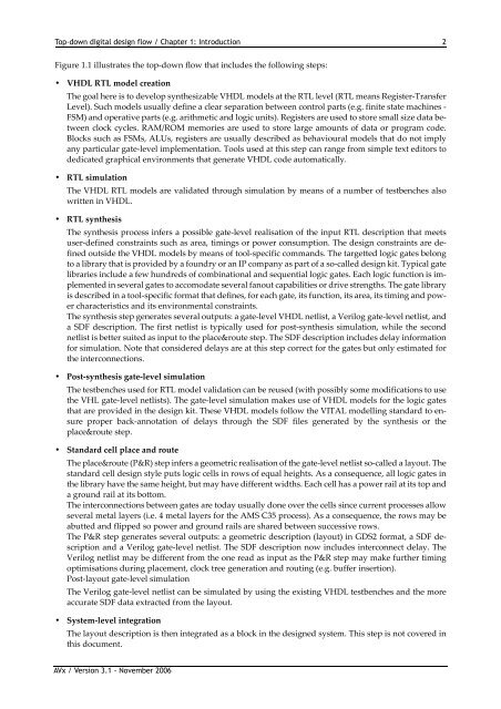
<strong>Top</strong>-<strong>down</strong> <strong>digital</strong> <strong>design</strong> <strong>flow</strong> / Chapter 1: Introduction 2Figure 1.1 illustrates the top‐<strong>down</strong> <strong>flow</strong> that includes the following steps:• VHDL RTL model creationThe goal here is to develop synthesizable VHDL models at the RTL level (RTL means Register‐TransferLevel). Such models usually define a clear separation between control parts (e.g. finite state machines ‐FSM) and operative parts (e.g. arithmetic and logic units). Registers are used to store small size data betweenclock cycles. RAM/ROM memories are used to store large amounts of data or program code.Blocks such as FSMs, ALUs, registers are usually described as behavioural models that do not implyany particular gate‐level implementation. Tools used at this step can range from simple text editors todedicated graphical environments that generate VHDL code automatically.• RTL simulationThe VHDL RTL models are validated through simulation by means of a number of testbenches alsowritten in VHDL.• RTL synthesisThe synthesis process infers a possible gate‐level realisation of the input RTL description that meetsuser‐defined constraints such as area, timings or power consumption. The <strong>design</strong> constraints are definedoutside the VHDL models by means of tool‐specific commands. The targetted logic gates belongto a library that is provided by a foundry or an IP company as part of a so‐called <strong>design</strong> kit. Typical gatelibraries include a few hundreds of combinational and sequential logic gates. Each logic function is implementedin several gates to accomodate several fanout capabilities or drive strengths. The gate libraryis described in a tool‐specific format that defines, for each gate, its function, its area, its timing and powercharacteristics and its environmental constraints.The synthesis step generates several outputs: a gate‐level VHDL netlist, a Verilog gate‐level netlist, anda SDF description. The first netlist is typically used for post‐synthesis simulation, while the secondnetlist is better suited as input to the place&route step. The SDF description includes delay informationfor simulation. Note that considered delays are at this step correct for the gates but only estimated forthe interconnections.• Post‐synthesis gate‐level simulationThe testbenches used for RTL model validation can be reused (with possibly some modifications to usethe VHL gate‐level netlists). The gate‐level simulation makes use of VHDL models for the logic gatesthat are provided in the <strong>design</strong> kit. These VHDL models follow the VITAL modelling standard to ensureproper back‐annotation of delays through the SDF files generated by the synthesis or theplace&route step.• Standard cell place and routeThe place&route (P&R) step infers a geometric realisation of the gate‐level netlist so‐called a layout. Thestandard cell <strong>design</strong> style puts logic cells in rows of equal heights. As a consequence, all logic gates inthe library have the same height, but may have different widths. Each cell has a power rail at its top anda ground rail at its bottom.The interconnections between gates are today usually done over the cells since current processes allowseveral metal layers (i.e. 4 metal layers for the AMS C35 process). As a consequence, the rows may beabutted and flipped so power and ground rails are shared between successive rows.The P&R step generates several outputs: a geometric description (layout) in GDS2 format, a SDF descriptionand a Verilog gate‐level netlist. The SDF description now includes interconnect delay. TheVerilog netlist may be different from the one read as input as the P&R step may make further timingoptimisations during placement, clock tree generation and routing (e.g. buffer insertion).Post‐layout gate‐level simulationThe Verilog gate‐level netlist can be simulated by using the existing VHDL testbenches and the moreaccurate SDF data extracted from the layout.• System‐level integrationThe layout description is then integrated as a block in the <strong>design</strong>ed system. This step is not covered inthis document.AVx / Version 3.1 - November 2006


