

Top-down digital design flow - Microelectronic Systems Laboratory
Top-down digital design flow - Microelectronic Systems Laboratory
Top-down digital design flow - Microelectronic Systems Laboratory

You also want an ePaper? Increase the reach of your titles
YUMPU automatically turns print PDFs into web optimized ePapers that Google loves.
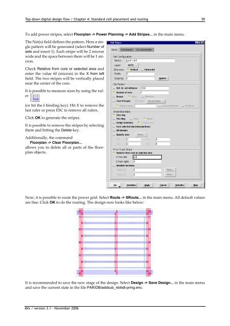
<strong>Top</strong>-<strong>down</strong> <strong>digital</strong> <strong>design</strong> <strong>flow</strong> / Chapter 4: Standard cell placement and routing 39To add power stripes, select Floorplan -> Power Planning -> Add Stripes... in the main menu.The Net(s) field defines the pattern. Here a singlepattern will be generated (select Number ofsets and insert 1). Each stripe will be 2 micronwide and the space between them will be 1 micron.Check Relative from core or selected area andenter the value 60 (micron) in the X from leftfield. The two stripes will be vertically placednear the center of the core.It is possible to measure sizes by using the ruler(or hit the k binding key). Hit K to remove thelast ruler or press ESC to remove all rulers.Click OK to generate the stripes.It is possible to remove the stripes by selectingthem and hitting the Delete key.Additionally, the commandFloorplan -> Clear Floorplan...allows you to delete all or parts of the floorplanobjects.Now, it is possible to route the power grid. Select Route -> SRoute... in the main menu. All default valuesare fine. Click OK to do the routing. The <strong>design</strong> now looks like below:It is recommended to save the new stage of the <strong>design</strong>. Select Design -> Save Design... in the main menuand save the current state in the file PAR/DB/addsub_nbits8-pring.enc.AVx / version 3.1 - November 2006


