Integrator/CP User Guide - ARM Information Center
Integrator/CP User Guide - ARM Information Center
Integrator/CP User Guide - ARM Information Center
You also want an ePaper? Increase the reach of your titles
YUMPU automatically turns print PDFs into web optimized ePapers that Google loves.
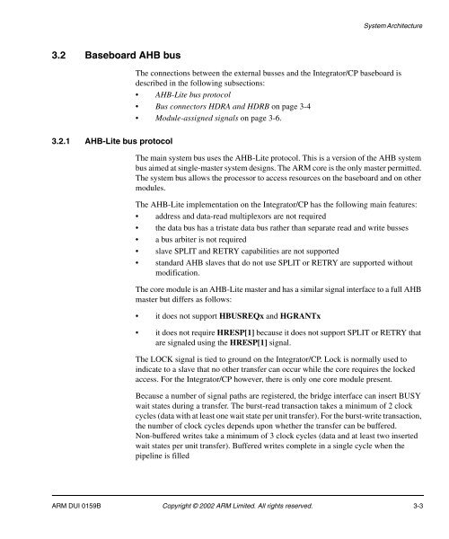
System Architecture3.2 Baseboard AHB busThe connections between the external busses and the <strong>Integrator</strong>/<strong>CP</strong> baseboard isdescribed in the following subsections:• AHB-Lite bus protocol• Bus connectors HDRA and HDRB on page 3-4• Module-assigned signals on page 3-6.3.2.1 AHB-Lite bus protocolThe main system bus uses the AHB-Lite protocol. This is a version of the AHB systembus aimed at single-master system designs. The <strong>ARM</strong> core is the only master permitted.The system bus allows the processor to access resources on the baseboard and on othermodules.The AHB-Lite implementation on the <strong>Integrator</strong>/<strong>CP</strong> has the following main features:• address and data-read multiplexors are not required• the data bus has a tristate data bus rather than separate read and write busses• a bus arbiter is not required• slave SPLIT and RETRY capabilities are not supported• standard AHB slaves that do not use SPLIT or RETRY are supported withoutmodification.The core module is an AHB-Lite master and has a similar signal interface to a full AHBmaster but differs as follows:• it does not support HBUSREQx and HGRANTx• it does not require HRESP[1] because it does not support SPLIT or RETRY thatare signaled using the HRESP[1] signal.The LOCK signal is tied to ground on the <strong>Integrator</strong>/<strong>CP</strong>. Lock is normally used toindicate to a slave that no other transfer can occur while the core requires the lockedaccess. For the <strong>Integrator</strong>/<strong>CP</strong> however, there is only one core module present.Because a number of signal paths are registered, the bridge interface can insert BUSYwait states during a transfer. The burst-read transaction takes a minimum of 2 clockcycles (data with at least one wait state per unit transfer). For the burst-write transaction,the number of clock cycles depends upon whether the transfer can be buffered.Non-buffered writes take a minimum of 3 clock cycles (data and at least two insertedwait states per unit transfer). Buffered writes complete in a single cycle when thepipeline is filled<strong>ARM</strong> DUI 0159B Copyright © 2002 <strong>ARM</strong> Limited. All rights reserved. 3-3


