

Integrator/CP User Guide - ARM Information Center
Integrator/CP User Guide - ARM Information Center
Integrator/CP User Guide - ARM Information Center

Create successful ePaper yourself
Turn your PDF publications into a flip-book with our unique Google optimized e-Paper software.
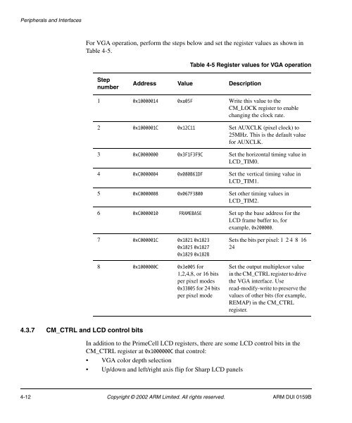
Peripherals and InterfacesFor VGA operation, perform the steps below and set the register values as shown inTable 4-5.Table 4-5 Register values for VGA operationStepnumberAddress Value Description1 0x10000014 0xa05F Write this value to theCM_LOCK register to enablechanging the clock rate.2 0x1000001C 0x12C11 Set AUXCLK (pixel clock) to25MHz. This is the default valuefor AUXCLK.3 0xC0000000 0x3F1F3F9C Set the horizontal timing value inLCD_TIM0.4 0xC0000004 0x080B61DF Set the vertical timing value inLCD_TIM1.5 0xC0000008 0x067F3800 Set other timing values inLCD_TIM2.6 0xC0000010 FRAMEBASE Set up the base address for theLCD frame buffer to, forexample, 0x200000.7 0xC000001C 0x1821 0x18230x1825 0x18270x1829 0x182B8 0x1000000C 0x3e005 for1,2,4,8, or 16 bitsper pixel modes0x33805 for 24 bitsper pixel modeSets the bits per pixel: 1 2 4 8 1624Set the output multiplexor valuein the CM_CTRL register to drivethe VGA interface. <strong>User</strong>ead-modify-write to preserve thevalues of other bits (for example,REMAP) in the CM_CTRLregister.4.3.7 CM_CTRL and LCD control bitsIn addition to the PrimeCell LCD registers, there are some LCD control bits in theCM_CTRL register at 0x1000000C that control:• VGA color depth selection• Up/down and left/right axis flip for Sharp LCD panels4-12 Copyright © 2002 <strong>ARM</strong> Limited. All rights reserved. <strong>ARM</strong> DUI 0159B


