

Integrator/CP User Guide - ARM Information Center
Integrator/CP User Guide - ARM Information Center
Integrator/CP User Guide - ARM Information Center

Create successful ePaper yourself
Turn your PDF publications into a flip-book with our unique Google optimized e-Paper software.
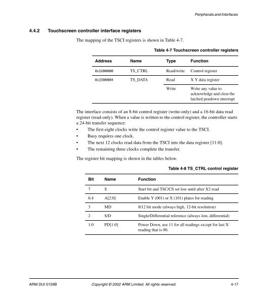
Peripherals and Interfaces4.4.2 Touchscreen controller interface registersThe mapping of the TSCI registers is shown in Table 4-7.Table 4-7 Touchscreen controller registersAddress Name Type Function0x1E000000 TS_CTRL Read/write Control register0x1E000004 TS_DATA Read X Y data registerWriteWrite any value toacknowledge and clear thelatched pendown interruptThe interface consists of an 8-bit control register (write-only) and a 16-bit data readregister (read-only). When a value is written to the control register, the controller startsa 24-bit transfer sequence:• The first eight clocks write the control register value to the TSCI.• Busy requires one clock.• The next 12 clocks read data from the TSCI into the data register [11:0].• The remaining three clocks complete the transfer.The register bit mapping is shown in the tables below.Bit Name FunctionTable 4-8 TS_CTRL control register7 S Start bit and TSC/CS set low until after X2 read6:4 A[2:0] Enable Y (001) or X (101) plates for reading3 MD 8/12 bit mode (always high, 12-bit resolution)2 S/D Single/Differential reference (always low, differential)1:0 PD[1:0] Power Down, use 11 for all readings except for last Xreading that is 00.<strong>ARM</strong> DUI 0159B Copyright © 2002 <strong>ARM</strong> Limited. All rights reserved. 4-17


