

Integrator/CP User Guide - ARM Information Center
Integrator/CP User Guide - ARM Information Center
Integrator/CP User Guide - ARM Information Center

You also want an ePaper? Increase the reach of your titles
YUMPU automatically turns print PDFs into web optimized ePapers that Google loves.
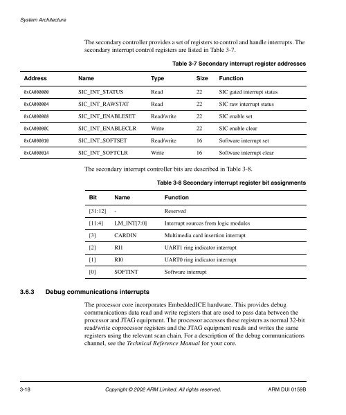
System ArchitectureThe secondary controller provides a set of registers to control and handle interrupts. Thesecondary interrupt control registers are listed in Table 3-7.Table 3-7 Secondary interrupt register addressesAddress Name Type Size Function0xCA000000 SIC_INT_STATUS Read 22 SIC gated interrupt status0xCA000004 SIC_INT_RAWSTAT Read 22 SIC raw interrupt status0xCA000008 SIC_INT_ENABLESET Read/write 22 SIC enable set0xCA00000C SIC_INT_ENABLECLR Write 22 SIC enable clear0xCA000010 SIC_INT_SOFTSET Read/write 16 Software interrupt set0xCA000014 SIC_INT_SOFTCLR Write 16 Software interrupt clearThe secondary interrupt controller bits are described in Table 3-8.Bit Name Function[31:12] - ReservedTable 3-8 Secondary interrupt register bit assignments[11:4] LM_INT[7:0] Interrupt sources from logic modules[3] CARDIN Multimedia card insertion interrupt[2] RI1 UART1 ring indicator interrupt[1] RI0 UART0 ring indicator interrupt[0] SOFTINT Software interrupt3.6.3 Debug communications interruptsThe processor core incorporates EmbeddedICE hardware. This provides debugcommunications data read and write registers that are used to pass data between theprocessor and JTAG equipment. The processor accesses these registers as normal 32-bitread/write coprocessor registers and the JTAG equipment reads and writes the sameregisters using the relevant scan chain. For a description of the debug communicationschannel, see the Technical Reference Manual for your core.3-18 Copyright © 2002 <strong>ARM</strong> Limited. All rights reserved. <strong>ARM</strong> DUI 0159B


