Script for Laboratory: Designing embedded ASIPs - CES
Script for Laboratory: Designing embedded ASIPs - CES
Script for Laboratory: Designing embedded ASIPs - CES

Create successful ePaper yourself
Turn your PDF publications into a flip-book with our unique Google optimized e-Paper software.
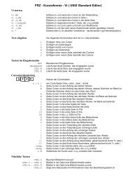
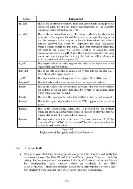
Signal Explanation<br />
im_data This is the Instruction Memory Data that corresponds to the previous<br />
shown im_addr. So it’s the binary representation of the assembly<br />
instruction that is fetched by the CPU.<br />
w_enb0 This is the write-enabled signal. It controls, whether the data at the<br />
input port of the register file will be written to the specified register or<br />
not. For example while jump or multicycle instructions this value is<br />
partially disabled (i.e. value ‘0’). Especially the jump instructions<br />
create a typical pattern <strong>for</strong> this signal. The jump instruction itself does<br />
not write to the register file, so this signal is ‘0’ when the jump<br />
instruction comes to its WB phase. The 2 instructions after the jump<br />
instruction enter the pipeline, but only the first one will be allowed to<br />
write its result back to the register file.<br />
w_sel0 This signal selects to which register the value at the input port of the<br />
register file shall be written.<br />
data_in0 This is the data value that is going to be written into the register file, if<br />
the write-enabled signal is active.<br />
r_selX This signal selects which register of the register file shall be read.<br />
data_outX This is the data value that was read from the requested register.<br />
dataab This is the Address Bus <strong>for</strong> memory accesses. This bus either contains<br />
the address to which some data shall be written or the address from<br />
which some data shall be read.<br />
datadb The Data Bus contains the value that shall be written or that was read.<br />
datareq This is the request signal with which the CPU triggers a read or a write<br />
access.<br />
dataack This is the acknowledge signal, that is activated by the memory<br />
controller after a requested write access is finished or after the data bus<br />
contains the result of a requested read access.<br />
datawin This signal determines the write mode. The usual values are “1111” <strong>for</strong><br />
“read word” and “0000” <strong>for</strong> “write word”, but there are also values <strong>for</strong><br />
writing 8- and 16-bit values.<br />
Figure 5-7<br />
Explanation of the signals in the ModelSim wave<br />
5.2 General hints<br />
• Change to your ModelSim directory inside your project directory tree and verify that<br />
the memory images TestData.IM and TestData.DM are present. They were build by<br />
mkimg. Furthermore you need the testbench file tb_ASIPmeister.vhd and the Model-<br />
Sim configuration script wave.do, which are available in the TEM-<br />
PLATE_PROJECT/ModelSim directory. Please check their existence in your Model-<br />
Sim directory be<strong>for</strong>e you start the work. It keeps you away from trouble.<br />
- 52 -