FIBEROPTIC SENSOR TECHNOLOGY HANDBOOK
FIBEROPTIC SENSOR TECHNOLOGY HANDBOOK
FIBEROPTIC SENSOR TECHNOLOGY HANDBOOK

You also want an ePaper? Increase the reach of your titles
YUMPU automatically turns print PDFs into web optimized ePapers that Google loves.
mately a 0.5 electron-volt increase. For fractional<br />
parts of Al greater than 0.37, i.e., x > 0.37, mechanisms<br />
in addition to simple photon production occur during<br />
recombination with the result that not all of the<br />
energy goes into producing photons, part of it goes into<br />
thermal energy with the possibility of crystal damage<br />
and a reduced tendency for lasing. The wavelength<br />
can be obtained from the photon energy relation E t<br />
= hf<br />
and from the wavelength-frequency-velocity relation ~f=<br />
= c/n, from which the relation 1 = hc/nEt is obtained,<br />
where h is Planck’s constant, c is the velocity of light<br />
in a vacuum, n is the refractive index taken as unity,<br />
and E t<br />
is the energy lost by a particle. For a particle<br />
with a charge of one electron that loses energy<br />
equal to the gap energy, A = 1.24/Eg, where h is the<br />
wavelength in microns and Eg is the gap energy in electron-volts.<br />
Thus for GaAs, 1 = 0.90 micron and for 37%<br />
Al, 1 = 0.64 micron. Longer wavelength lasers (1.1<br />
micron to 1.6 micron) can be produced by using the<br />
quarternary alloy iridium-gallium-arsenic-phosphorous<br />
(InGaAsP).<br />
1 P,<br />
A —P —~ qi - N—<br />
I<br />
I<br />
I<br />
I<br />
1<br />
1<br />
++++++++++++++++++++++++++<br />
I<br />
1<br />
Gal.xA~As:Ge ,~Ga l-y A’yAs ~ Gal_xAlxAs:Sn/Te<br />
I<br />
Ge ‘<br />
S;;Te<br />
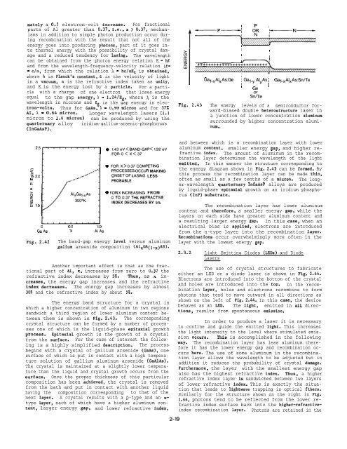
Fig. 2.43 The energy levels of a semiconductor forward-biased<br />
double heterostructure laser in<br />
a junction of lower concentration alumlnum<br />
surrounded by higher concentration aluminum.<br />
‘“’~ “’:;’v:;:N:;GAp0.37COMPETING<br />
9 /.<br />
~ ,- PROCESSES OCCUR MAKING<br />
/-<br />
m2.O<br />
u ...” ONSET OF LASING LESS<br />
..0” PROBABLE<br />
n-<br />
a<br />
><br />
0 AIXGal.XAs ● FOR X INCREASING FROM<br />
OT00.37 THE REFRACTIVE<br />
%<br />
300”K<br />
z<br />
INDEX DECREASES BY 5%<br />
u.1 15<br />
[1111111111<br />
o 0.5 1.0<br />
GaAs x AIAs<br />
Fig. 2.42<br />
The band-gap energy level versus aluminum<br />
galium arsenide composition (AIXGA(l-X)AS).<br />
Another important effect is that as the fractional<br />
part of Al, x, increases from zero to 0.37 the<br />
refractive index decreases by 5%. Thus, as x increases,<br />
the energy gap increases and the refractive<br />
index decreases. The energy gap increases by almost<br />
30% and the refractive index by about 5%.<br />
The energy band structure for a crystal in<br />
which a higher concentration of aluminum in two regions<br />
sandwich a third region of lower aluminum content between<br />
them is shown in Fig. 2.43. The corresponding<br />
crystal structure can be formed by a number of processes<br />
one of which is the liquid-phase epitaxial growth<br />
process. Epitaxial growth is the growth of a crystal<br />
from the surface. For the case of interest the following<br />
is a highly simplified description. The process<br />
begins with a crystal of gallium arsenide (GaAs), one<br />
surface of which is put in contact with a high temperature<br />
solution of gallium aluminum arsenide (GaAIAs).<br />
The crystal is maintained at a slightly lower temperature<br />
than the liquid and crystal growth occurs from the<br />
surface. Once the proper thickness of this particular<br />
composition has been achieved, the crystal is removed<br />
from the bath and put in contact with another liquid<br />
having the composition corresponding to that of the<br />
next layer. A crystal results with a p-type and an n-<br />
type layer, each of which have a higher aluminum content,<br />
larger energy gap, and lower refractive index,<br />
2-19<br />
and between which is a recombination layer with lower<br />
aluminum content, smaller energy gap, and higher refractive<br />
index. The amount of aluminum in the recombination<br />
layer determines the wavelength of the light<br />
emitted. In this manner the structure corresponding to<br />
the energy diagram shown in Fig. 2.43 can be formed. By<br />
this process the recombination layer can be made thin,<br />
often as small as a few tenths of a micron. The longer-wavelength<br />
quarternary InGaAsP alloys are produced<br />
by liquid-phase epitaxial growth on an iridium phosphorus<br />
(InP) substrate.<br />
The recombination layer has lower aluminum<br />
content and therefore, a smaller energy gap, while the<br />
layers on each side have greater aluminum content and<br />
a resulting larger energy gap. In this case, when an<br />
electrical bias is applied, electrons are introduced<br />
from the n-type layer into the recombination layer.<br />
Recombination occur overwhelmingly more often in the<br />
layer with the lowest energy gap.<br />
2.3.2 Light Emitting Diodes (LEDs) and Diode<br />
Lasers<br />
The use of crystal structures to fabricate<br />
either an LED or a diode laser is shown in Fig. 2.44.<br />
Electrons are introduced into the bottom of the crystal<br />
and holes are introduced into the top. In the recombination<br />
layer, holes and electrons recombine to form<br />
photons that tend to move outward in all directions as<br />
shown on the left of Fig. 2.44. In this case, the device<br />
behaves as an LED. The light, emitted in all directions,<br />
results from spontaneous emission.<br />
In order to produce a laser it is necessary<br />
to confine and guide the emitted light. This increases<br />
the light intensity to the level where stimulated emission<br />
occurs. This is accomplished in the following<br />
way. The recombination layer has less aluminum therefore<br />
it has the lower energy gap and recombination occurs<br />
here. The use of some aluminum in the recombination<br />
layer allows the wavelength to be adjusted but in<br />
addition it reduces the probability of crystal damage.<br />
Furthermore, the layer with the smallest energy gap<br />
also has the highest refractive index. Thus, a higher<br />
refractive index layer is sandwiched between two layers<br />
of lower refractive index. This is exactly the situation<br />
that leads to lightwave trapping in optical fibers.<br />
Similarly for the structure shown on the right in Fig.<br />
2.44, photons tend to be reflected from the lower refractive<br />
index surface back into the higher-refractiveindex<br />
recombination layer. Photons are retained in the