FIBEROPTIC SENSOR TECHNOLOGY HANDBOOK
FIBEROPTIC SENSOR TECHNOLOGY HANDBOOK
FIBEROPTIC SENSOR TECHNOLOGY HANDBOOK

Create successful ePaper yourself
Turn your PDF publications into a flip-book with our unique Google optimized e-Paper software.
4.3 INTEGRATED OPTICAL CIRCUITS (IOCS)<br />
The optical counterpart of the field of integrated<br />
electronics is the field of integrated optics.<br />
However, though integrated optical circuita have been<br />
made, they are for the moat part not commercially<br />
available. They are the subject of extensive research<br />
and development efforta at a large number of laboratories.<br />
The goal of these efforts is to commercially fabricate<br />
in large quantities these miniaturized devices<br />
with interconnected waveguides all on a single substrate.<br />
The generation, detection, propagation, modulation,<br />
switching, and coupling of light on such substrates<br />
have been accomplished. Techniques for the<br />
fabrication of substrates and the production of the<br />
high resolution material distribution patterns required<br />
for these integrated optical circuits exist. Most<br />
integrated optical circuits and associated devicea<br />
operate in a singlemode, therefore they are compatible<br />
with singlemode optical fibers. In essence most LEDs,<br />
diode lasers, and photodiodea are integrated optic<br />
devices. Integrated optical circuits are considered<br />
here because they are a part of second generation fiberoptic<br />
sensor technology.<br />
The waveguides used in integrated optical<br />
circuits are usually of two types namely planar films,<br />
that confine the light wavea in the vertical direction,<br />
and planar strips, (channels) that confine lightwaves<br />
in two dimensions. In both caaea, the waveguides are<br />
made of a higher refractive index than the surrounding<br />
material. Light is trapped in the layer or channel in<br />
much the same way that it is trapped in the core of an<br />
optical fiber. These planar waveguides can be formed<br />
by sputtering glass on a substrate of lower refractive<br />
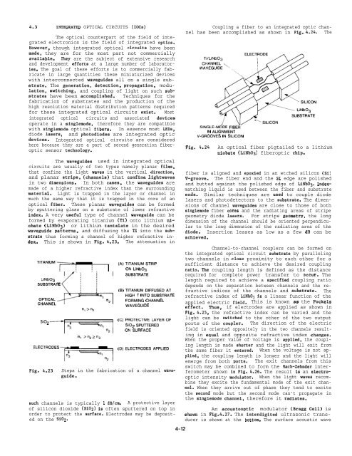
index. A very uaeful type of channel waveguide can be<br />
formed by evaporating titanium (Ti) onto lithium niobate<br />
(LiNb03) or lithium tantalate in the desired<br />
waveguide patterns, and diffusing the Ti into the aubstrate<br />
thus forming a channel of higher refractive index.<br />
This is shown in Fig. 4.23. The attenuation in<br />
“’’”’””-r<br />
LiNb03<br />
SUBSTRATE<br />
“1<br />
OPTICAL<br />
n2<br />
CHANNEL&<br />
nl>nz<br />
Si02_<br />
ELECTRODES—<br />
Fig. 4.23<br />
n1>n2>n3<br />
(A) TITANIUM STRIP<br />
ON LiNb03<br />
SUBSTRATE<br />
(B) TITANIUM DIFFUSEDAT<br />
HIGH T INTO SUBSTRATE<br />
FORMING CHANNEL<br />
WAVEGUIDE<br />
(C) PROTECTIVE LAYEROF<br />
Si02 SPUTTERED<br />
ON SURFACE<br />
(D) ELECTRODES APPLIED<br />
Steps in the fabrication of a channel waveguide.<br />
auch channels is typically 1 dB/cm. A protective layer<br />
of silicon dioxide (Si02) ia often sputtered on top in<br />
order to protect the surface. Electrodes may be deposited<br />
on the Si02.<br />
Coupling a fiber to an integrated optic channel<br />
has been accomplished as shown in Fig. 4.24. The<br />
1 v “’SILICON<br />
SINGLE-MODE FIBEti<br />
IN ALIGNMENT<br />
V-GROOVES IN SILICON<br />
Fig. 4.24<br />
An optical fiber pigtailed to a lithium<br />
niobate (LiNb03) fiberoptic chip.<br />
fiber is aligned and epoxied in an etched silicon (Si)<br />
V-groove. The fiber end and the Si edge are polished<br />
and butted against the polished edge of LiNb03. Indexmatching<br />
liquid is used between the fiber and substrate<br />
ends. Similar techniques are uaed to couple diode<br />
lasers and photodetectors to the substrate. The dimensions<br />
of channel waveguides are close to those of both<br />
ainglemode fiber corea and the radiating areas of stripe<br />
geometry diode lasers. For stripe geometry, the long<br />
dimension of the channel should be oriented perpendicular<br />
to the long dimension of the radiating area of the<br />
diode. Insertion leases as low as a few dB can be<br />
achieved.<br />
Channel-to-channel couplers can be formed on<br />
the integrated optical circuit aubstrate by paralleling<br />
two channels in cloae proximity to each other for a<br />
sufficient distance to achieve the desired coupling<br />
ratio. The coupling length is defined as the distance<br />
required for complete power transfer to occur. The<br />
length required to achieve a apecified coupling ratio<br />
depends on the separation between channels and the refractive<br />
indices of the channels and subatrate. The<br />
refractive index of LiNb03 ia a linear function of the<br />
applied electric field. This is known aa the Pockels<br />
effect. Thus, if electrodes are applied as shown in<br />
Fig. 4.25, the refractive index can be varied and the<br />
light can be awitched to the other of the two output<br />
ports of the coupler. The direction of the electric<br />
field is oriented oppositely in the two channels resulting<br />
in equal and opposite refractive index changes.<br />
When the proper value of voltage is applied, the coupling<br />
length is made ahorter and the light will exit from<br />
the same fiber it entered. When the voltage is not applied,<br />
the coupling length is longer and the light will<br />
emerge from both ports. The exit channels from this<br />
switch may be combined to form the Mach-Zehnder interferometer<br />
shown in Fig. 4.26. The result is an electrooptic<br />
intensity modulator. When the light wavea recombine<br />
they excite the fundamental mode of the exit channel.<br />
When they arrive out of phase they tend to excite<br />
the aecond mode but the second mode can’t propagate in<br />
the singlemode channel, therefore it radiatea.<br />
An acoustooptic modulator (Bragg Cell) is<br />
ahown in Fig. 4.27. The interdigited ultrasonic transducer<br />
is shown at the bottom. The surface acoustic wave<br />
4-12