Local polarization dynamics in ferroelectric materials
Local polarization dynamics in ferroelectric materials
Local polarization dynamics in ferroelectric materials

Create successful ePaper yourself
Turn your PDF publications into a flip-book with our unique Google optimized e-Paper software.
Rep. Prog. Phys. 73 (2010) 056502<br />
S V Kal<strong>in</strong><strong>in</strong> et al<br />
(a) 1 µm (b) (c)<br />
10<br />
x 2 , ξ 2<br />
L<br />
E 3<br />
P S<br />
DW<br />
P S<br />
x 1 , ξ 1<br />
H<br />
Width/H<br />
1<br />
3<br />
2<br />
x 3 , ξ 3<br />
0.1<br />
1<br />
(d)<br />
(e)<br />
10 -2 0.1 1 10<br />
L/H<br />
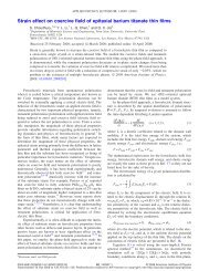
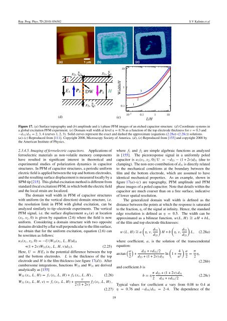
Figure 17. (a) Surface topography and (b) amplitude and (c) phase PFM images of an etched capacitor structure. (d) Coord<strong>in</strong>ate systems <strong>in</strong><br />
a global excitation PFM experiment. (e) Doma<strong>in</strong> wall width at level η = 0.76 as a function of the top electrode thickness for ν = 0.3 and<br />
−d 33 /d 31 = 2, 3, 4 (curves 1, 2, 3). Solid curves represent the exact and dashed the approximate (equations (2.28a)–(2.28c)) solutions.<br />
(a)–(c) Reproduced from [111]. Copyright 2008, Microscopy Society of America. (d), (e) Reproduced from [155] and copyright 2008 by<br />
the American Institute of Physics.<br />
2.3.4.5. Imag<strong>in</strong>g of <strong>ferroelectric</strong> capacitors. Applications of<br />
<strong>ferroelectric</strong> <strong>materials</strong> as non-volatile memory components<br />
have resulted <strong>in</strong> significant <strong>in</strong>terest <strong>in</strong> theoretical and<br />
experimental studies of <strong>polarization</strong> <strong>dynamics</strong> <strong>in</strong> capacitor<br />
structures. In PFM of capacitor structures, a periodic uniform<br />
electric field is applied between the top and bottom electrodes,<br />
and the result<strong>in</strong>g surface displacement is measured locally by a<br />
SPM tip [215]. This global excitation method is different from<br />
standard (local excitation) PFM, <strong>in</strong> which both the electric field<br />
and the local stra<strong>in</strong> are localized.<br />
The doma<strong>in</strong> wall width <strong>in</strong> PFM of capacitor structures<br />
with uniform (<strong>in</strong> the vertical direction) doma<strong>in</strong> structure, i.e.<br />
the resolution limit <strong>in</strong> PFM with global excitation, can be<br />
analyzed similarly to tip–electrode experiments. The vertical<br />
PFM signal, i.e. the surface displacement u 3i (x) at location<br />
(x 1 ,x 2 , 0) is given by equation (2.6) where the field is now<br />
uniform. Consider<strong>in</strong>g a doma<strong>in</strong> structure with two opposite<br />
doma<strong>in</strong>s divided by a flat wall perpendicular to the film surface,<br />
we obta<strong>in</strong> that for the uniform excitation, equation (2.6) can<br />
be rewritten as follows:<br />
u 3 (x 1 ,x 2 , 0) =−U(W 33 (x 1 ,L,H)d 33<br />
+(1+2ν)W 31 (x 1 ,L,H,ν)d 31 ). (2.25)<br />
Here, U = HE 3 is the potential difference between the top<br />
and the bottom electrodes. L is the thickness of the top<br />
electrode and H is the film thickness (see figure 17(d)). After<br />
cumbersome <strong>in</strong>tegrations, functions W 33 and W 31 are derived<br />
analytically as [155]<br />
W 33 (x 1 ,L,H) = f 1 (x 1 ,L,H) + f 2 (x 1 ,L,H) , (2.26)<br />
ν<br />
W 31 (x 1 ,L,H,ν) = f 1 (x 1 ,L,H) +<br />
2 (1+2ν) f 2 (x 1 ,L,H) ,<br />
(2.27)<br />
where f 1 and f 2 are simple algebraic functions as analyzed<br />
<strong>in</strong> [155]. The piezoresponse signal <strong>in</strong> a uniformly poled<br />
capacitor is u 3 (x 1 ,x 2 , 0)/U = −d 33 − (1+2ν)d 31 (due to<br />
clamp<strong>in</strong>g). The non-zero contribution of d 31 is directly related<br />
to the mechanical conditions at the boundary between the<br />
film and the bottom electrode, which are assumed to have<br />
identical mechanical properties. As an example, shown <strong>in</strong><br />
figure 17(a)–(c) are topography, PFM amplitude and PFM<br />
phase images of a poled capacitor. Note that details with<strong>in</strong> the<br />
capacitor are much coarser than on a free surface, <strong>in</strong>dicative<br />
of lower spatial resolution.<br />
The generalized doma<strong>in</strong> wall width is def<strong>in</strong>ed as the<br />
distance between the po<strong>in</strong>ts at which the response is saturated<br />
to the fraction, η, of the signal at <strong>in</strong>f<strong>in</strong>ity. Hence, the standard<br />
edge resolution is def<strong>in</strong>ed as η = 0.5. The width can be<br />
approximated as a bil<strong>in</strong>ear function, w(L, H) ∼ = aH + bL,<br />
of the film and top electrode thicknesses:<br />
(<br />
w (L, H) ∼ = a η, ν, d ) (<br />
31<br />
H + b η, ν, d )<br />
31<br />
L, (2.28a)<br />
d 33 d 33<br />
where coefficient, a, is the solution of the transcendental<br />
equation:<br />
( a<br />
)<br />
arctan +<br />
2<br />
and coefficient b is<br />
(<br />
d 33 + νd 31 /2<br />
ln 1+ 4 ) a<br />
d 33 + (1+2ν) d 31 a 2 2 = π 2 η, (2.28b)<br />
b = η π 2<br />
d 33 + (1+2ν) d 31<br />
. (2.28c)<br />
d 33 + νd 31 /2<br />
Typical values for coefficient a vary from 0.08 to 0.4 at<br />
η = 0.76 and −d 33 /d 31 = 2–4. The dependence of the<br />
19