Local polarization dynamics in ferroelectric materials
Local polarization dynamics in ferroelectric materials
Local polarization dynamics in ferroelectric materials

You also want an ePaper? Increase the reach of your titles
YUMPU automatically turns print PDFs into web optimized ePapers that Google loves.
Rep. Prog. Phys. 73 (2010) 056502<br />
S V Kal<strong>in</strong><strong>in</strong> et al<br />
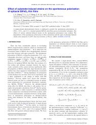
Response, a.u.<br />
1.0<br />
0.5<br />
0.0<br />
-0.5<br />
-1.0<br />
(a)<br />
-10 -5 0 5 10<br />
Bias, V dc<br />
Work of switch<strong>in</strong>g, a.u. V<br />
(b)<br />
15<br />
10<br />
5<br />
0<br />
0 2 4 6 8 10<br />
Modulation voltage, V ac<br />
1.5<br />
1.0<br />
0.5<br />
0.0<br />
Switchable response, a.u.<br />
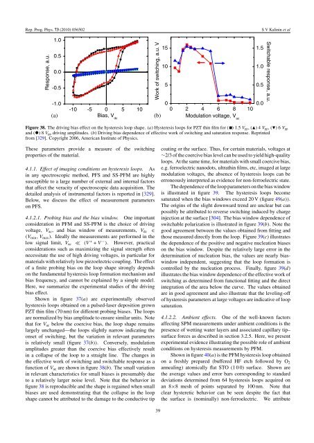
Figure 38. The driv<strong>in</strong>g bias effect on the hysteresis loop shape. (a) Hysteresis loops for PZT th<strong>in</strong> film for ( ) 1.5 V pp ,() 4V pp ,()6V pp<br />
and (•) 8V pp driv<strong>in</strong>g amplitudes. (b) Driv<strong>in</strong>g bias dependence of effective work of switch<strong>in</strong>g and saturation response. Repr<strong>in</strong>ted<br />
from [329]. Copyright 2006, American Institute of Physics.<br />
These parameters provide a measure of the switch<strong>in</strong>g<br />
properties of the material.<br />
4.1.1. Effect of imag<strong>in</strong>g conditions on hysteresis loops. As<br />
<strong>in</strong> any spectroscopic method, PFS and SS-PFM are highly<br />
susceptible to a large number of external and <strong>in</strong>ternal factors<br />
that affect the veracity of spectroscopic data acquisition. The<br />
detailed analysis of <strong>in</strong>strumental factors is reported <strong>in</strong> [329].<br />
Below, we discuss the effect of measurement parameters<br />
on PFS.<br />
4.1.2.1. Prob<strong>in</strong>g bias and the bias w<strong>in</strong>dow. One important<br />
consideration <strong>in</strong> PFM and SS-PFM is the choice of driv<strong>in</strong>g<br />
voltage, V ac , and bias w<strong>in</strong>dow of measurements, V dc ∈<br />
(V m<strong>in</strong> ,V max ). Ideally the measurements are performed <strong>in</strong> the<br />
low signal limit, V ac ≪ (V + + V − ). However, practical<br />
considerations such as maximiz<strong>in</strong>g the signal strength often<br />
necessitate the use of high driv<strong>in</strong>g voltages, <strong>in</strong> particular for<br />
<strong>materials</strong> with relatively low piezoelectric coupl<strong>in</strong>g. The effect<br />
of a f<strong>in</strong>ite prob<strong>in</strong>g bias on the loop shape strongly depends<br />
on the fundamental hysteresis loop formation mechanism and<br />
bias frequency, and cannot be expla<strong>in</strong>ed by a simple model.<br />
Here, we summarize the experimental studies of the driv<strong>in</strong>g<br />
bias effect.<br />
Shown <strong>in</strong> figure 37(a) are experimentally observed<br />
hysteresis loops obta<strong>in</strong>ed on a pulsed-laser deposition grown<br />
PZT th<strong>in</strong> film (70 nm) for different prob<strong>in</strong>g biases. The loops<br />
are normalized by bias amplitude to ensure similar units. Note<br />
that for V ac below the coercive bias, the loop shape rema<strong>in</strong>s<br />
largely unchanged—the loops slightly narrow <strong>in</strong>dicat<strong>in</strong>g the<br />
onset of switch<strong>in</strong>g, but the variation <strong>in</strong> relevant parameters<br />
is relatively small (figure 37(b)). Conversely, modulation<br />
amplitudes greater than the coercive bias effectively result<br />
<strong>in</strong> a collapse of the loop to a straight l<strong>in</strong>e. The changes <strong>in</strong><br />
the effective work of switch<strong>in</strong>g and switchable response as a<br />
function of V ac are shown <strong>in</strong> figure 38(b). The small variation<br />
<strong>in</strong> relevant characteristics for small biases is presumably due<br />
to a relatively larger noise level. Note that the behavior <strong>in</strong><br />
figure 38 is reproducible and the shape is rega<strong>in</strong>ed when small<br />
biases are used demonstrat<strong>in</strong>g that the collapse <strong>in</strong> the loop<br />
shape cannot be attributed to the damage to the conductive tip<br />
coat<strong>in</strong>g or the surface. Thus, for certa<strong>in</strong> <strong>materials</strong>, voltages at<br />
∼2/3 of the coercive bias level can be used to yield high-quality<br />
loops. At the same time, for <strong>materials</strong> with small coercive bias,<br />
e.g. <strong>ferroelectric</strong> nanodots, ultrath<strong>in</strong> films, etc, imaged at large<br />
modulation voltages, the absence of hysteresis loops can be<br />
erroneously <strong>in</strong>terpreted as evidence for non-<strong>ferroelectric</strong> state.<br />
The dependence of the loop parameters on the bias w<strong>in</strong>dow<br />
is illustrated <strong>in</strong> figure 39. The hysteresis loops become<br />
saturated when the bias w<strong>in</strong>dows exceed 20 V (figure 49(a)).<br />
The orig<strong>in</strong>s of the slight downward trend are unclear but can<br />
possibly be attributed to reverse switch<strong>in</strong>g <strong>in</strong>duced by charge<br />
<strong>in</strong>jection at the surface [304]. The bias w<strong>in</strong>dow dependence of<br />
switchable <strong>polarization</strong> is illustrated <strong>in</strong> figure 39(b). Note the<br />
good agreement between the values obta<strong>in</strong>ed from fitt<strong>in</strong>g and<br />
those measured directly from the loop. Figure 39(c) illustrates<br />
the dependence of the positive and negative nucleation biases<br />
on the bias w<strong>in</strong>dow. Despite the relatively large error <strong>in</strong> the<br />
determ<strong>in</strong>ation of nucleation bias, the values are nearly biasw<strong>in</strong>dow<br />
<strong>in</strong>dependent, suggest<strong>in</strong>g that the loop formation is<br />
controlled by the nucleation process. F<strong>in</strong>ally, figure 39(d)<br />
illustrates the bias w<strong>in</strong>dow dependence of the effective work of<br />
switch<strong>in</strong>g as determ<strong>in</strong>ed from functional fitt<strong>in</strong>g and the direct<br />
<strong>in</strong>tegration of the area below the curve. The values obta<strong>in</strong>ed<br />
are <strong>in</strong> good agreement and also illustrate that the level<strong>in</strong>g-off<br />
of hysteresis parameters at large voltages are <strong>in</strong>dicative of loop<br />
saturation.<br />
4.1.2.2. Ambient effects. One of the well-known factors<br />
affect<strong>in</strong>g SPM measurements under ambient conditions is the<br />
presence of wett<strong>in</strong>g water layers and associated capillary tip–<br />
surface forces as described <strong>in</strong> section 3.2.5. Here, we present<br />
experimental evidence illustrat<strong>in</strong>g the possible role of ambient<br />
conditions on hysteresis measurements by PFM.<br />
Shown <strong>in</strong> figure 40(a) is the PFM hysteresis loop obta<strong>in</strong>ed<br />
on a freshly prepared (buffered HF etch followed by O 2<br />
anneal<strong>in</strong>g) atomically flat STO (1 0 0) surface. Shown are<br />
the average values and error bars correspond<strong>in</strong>g to standard<br />
deviations determ<strong>in</strong>ed from 64 hysteresis loops acquired on<br />
an 8×8 mesh of po<strong>in</strong>ts separated by 100 nm. Note that<br />
clear hysteretic behavior can be seen despite the fact that<br />
the surface is (nom<strong>in</strong>ally) non-<strong>ferroelectric</strong>. We attribute<br />
39