Local polarization dynamics in ferroelectric materials
Local polarization dynamics in ferroelectric materials
Local polarization dynamics in ferroelectric materials

Create successful ePaper yourself
Turn your PDF publications into a flip-book with our unique Google optimized e-Paper software.
Rep. Prog. Phys. 73 (2010) 056502<br />
S V Kal<strong>in</strong><strong>in</strong> et al<br />
High Low<br />
ττ τ<br />
2<br />
1<br />
Amplitude<br />
(a)<br />
Time<br />
(b)<br />
Vac<br />
δτ<br />
τ 3<br />
V<br />
tip<br />
= V<br />
dc<br />
+ V<br />
ac<br />
s<strong>in</strong>ωt<br />
−<br />
V c<br />
−<br />
R 0<br />
Response<br />
+<br />
R s<br />
−<br />
R<br />
R <strong>in</strong>it<br />
−<br />
V c<br />
Bias<br />
(c)<br />
−<br />
R s<br />
(d)<br />
−<br />
R 0<br />
+<br />
V c<br />
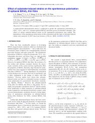
Figure 37. (a) Switch<strong>in</strong>g and (b) prob<strong>in</strong>g waveforms <strong>in</strong> SS-PFM. (c) Data acquisition sequence. (d) Schematics of well-saturated<br />
electromechanical hysteresis loop <strong>in</strong> the PFM experiment. Forward and reverse coercive voltages, V + and V − , nucleation voltages, V<br />
c<br />
+ and<br />
Vc −,<br />
forward and reverse saturation and remanent responses, R+ 0 , R− 0 , R+ s and R− s , are shown. Also shown is the <strong>in</strong>itial response, R <strong>in</strong>it. The<br />
work of switch<strong>in</strong>g A s is def<strong>in</strong>ed as the area with<strong>in</strong> the loop. The impr<strong>in</strong>t bias and maximum switchable <strong>polarization</strong> are def<strong>in</strong>ed as<br />
Im = V<br />
0 + − V −<br />
0<br />
and R m = R<br />
s + − R− s<br />
correspond<strong>in</strong>gly. Adapted with permission from [328]. Copyright 2006, American Institute of Physics.<br />
hysteresis loops. This approach was later used by<br />
several groups to probe crystallographic orientation and<br />
microstructure effects on switch<strong>in</strong>g behavior [157, 162, 324–<br />
327]. Recently, PFM spectroscopy has been extended to<br />
an imag<strong>in</strong>g mode us<strong>in</strong>g an algorithm for fast (30–100 ms)<br />
hysteresis loop measurements developed by Jesse et al [328].<br />
In the switch<strong>in</strong>g spectroscopy PFM (SS-PFM), hysteresis<br />
loops are acquired at each po<strong>in</strong>t of the image and analyzed<br />
to yield 2D maps of impr<strong>in</strong>t, coercive bias and work of<br />
switch<strong>in</strong>g, provid<strong>in</strong>g a comprehensive description of the<br />
switch<strong>in</strong>g behavior of the material at each po<strong>in</strong>t.<br />
Below, we summarize the technical aspects of voltage and<br />
time spectroscopy <strong>in</strong> PFM, discuss relevant theoretical aspects<br />
and summarize recent experimental advances.<br />
4.1. Experimental apparatus for PFS and SS-PFM<br />
Dur<strong>in</strong>g the acquisition of a hysteresis loop piezoresponse force<br />
spectroscopy (PFS), the tip is fixed at a given location on<br />
the surface and the waveform V tip = V probe (t) + V ac cos ωt<br />
is applied to the tip. V ac is the amplitude of the PFM driv<strong>in</strong>g<br />
signal. The prob<strong>in</strong>g signal, V probe (t), is shown <strong>in</strong> figure 37 and<br />
is composed of a sequence of pulses with amplitude, V i , and<br />
length, τ 1 (HIGH state) separated by <strong>in</strong>tervals of zero bias last<strong>in</strong>g<br />
for τ 2 (LOW state). The measured responses yield on-field and<br />
off-field hysteresis loops.<br />
To generate SS-PFM maps, the hysteresis loops are<br />
acquired over M × M po<strong>in</strong>t mesh with spac<strong>in</strong>g, l, between<br />
po<strong>in</strong>ts. The hysteresis curves are collected at each po<strong>in</strong>t and<br />
stored <strong>in</strong> a 3D data array for subsequent analysis. Parameters<br />
describ<strong>in</strong>g the switch<strong>in</strong>g process such as positive and negative<br />
coercive bias, impr<strong>in</strong>t voltage and saturation response can<br />
be extracted from the data sets and plotted as 2D maps;<br />
alternatively, hysteresis loops from selected po<strong>in</strong>t(s) can be<br />
extracted and analyzed.<br />
An ideal hysteresis loop for electromechanical measurements<br />
is shown <strong>in</strong> figure 37(d). Acquired at each po<strong>in</strong>t is<br />
a hysteresis loop conta<strong>in</strong><strong>in</strong>g the forward, R + (V ), and reverse,<br />
R − (V ), branches. The zero of R + (V ) def<strong>in</strong>es positive coercive<br />
bias, V + , and the zero of R − (V ) def<strong>in</strong>es negative coercive bias,<br />
V − . The impr<strong>in</strong>t is def<strong>in</strong>ed as Im = (V + + V − )/2. The values<br />
of R<br />
0 + = R+ (0) and R − 0<br />
= R− (0) def<strong>in</strong>e positive and negative<br />
remanent responses, while R 0 = R<br />
0 + − R− 0<br />
is the remanent<br />
switchable response. F<strong>in</strong>ally, R + (+∞) = R − (+∞) = R s<br />
+<br />
and R + (−∞) = R − (−∞) = Rs<br />
− are the saturation responses<br />
and R s = R s + − R− s is the maximal switchable response. In<br />
some cases, contributions of electrostatic signals (tip electrode)<br />
or bimorph-like substrate bend<strong>in</strong>g (macroscopic capacitors)<br />
necessitate the <strong>in</strong>troduction of vertical offset to symmetrize<br />
the loop. F<strong>in</strong>ally, the forward and reverse doma<strong>in</strong> nucleation<br />
voltages, V c<br />
+ and Vc − , correspond<strong>in</strong>g to the cross-over<br />
between constant and rapidly chang<strong>in</strong>g regions of the loop,<br />
are attributable to doma<strong>in</strong> nucleation below the tip. Additionally,<br />
the effective work of switch<strong>in</strong>g is def<strong>in</strong>ed as the area with<strong>in</strong><br />
a hysteresis loop,<br />
A s =<br />
∫ +∞<br />
−∞<br />
(<br />
R + (V ) − R − (V ) ) dV. (4.1)<br />
38