Local polarization dynamics in ferroelectric materials
Local polarization dynamics in ferroelectric materials
Local polarization dynamics in ferroelectric materials

Create successful ePaper yourself
Turn your PDF publications into a flip-book with our unique Google optimized e-Paper software.
Rep. Prog. Phys. 73 (2010) 056502<br />
S V Kal<strong>in</strong><strong>in</strong> et al<br />
d33 eff (pm/V)<br />
40<br />
20<br />
0<br />
-20<br />
-40<br />
(a)<br />
4 a/2<br />
Thickness h decrease<br />
3<br />
P S<br />
2 P S<br />
1<br />
a/2<br />
-P S<br />
-P S<br />
0 1 2 3 4<br />
2y 1 /a<br />
y 2<br />
h<br />
y 1<br />
P S -P S<br />
y 3<br />
(b)<br />
10 2 10 -3 10 -2 0.1 1 10<br />
d33 eff (pm/V)<br />
10<br />
1<br />
0.1<br />
(c)<br />
noise<br />
10 -3 10 -2 0.1 1 10<br />
h/d<br />
4<br />
1<br />
5<br />
2<br />
Doma<strong>in</strong> width<br />
a decrease<br />
3<br />
10 2 (d)<br />
4<br />
3<br />
10<br />
1<br />
0.1<br />
noise<br />
a/2d<br />
2<br />
Thickness h<br />
decrease<br />
1<br />
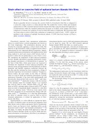
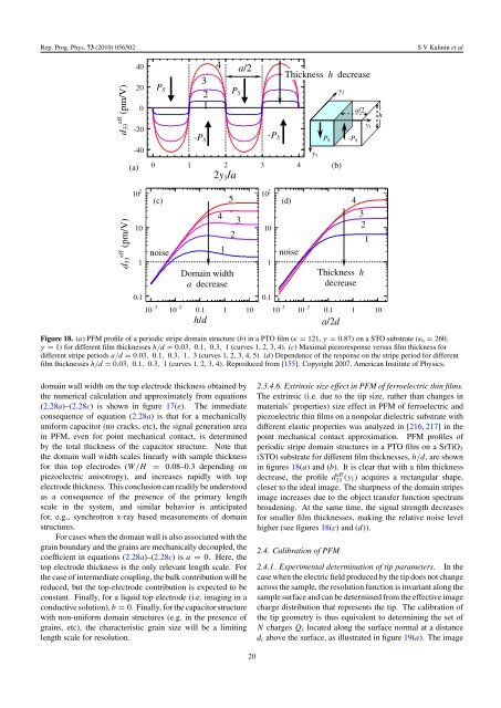
Figure 18. (a) PFM profile of a periodic stripe doma<strong>in</strong> structure (b) <strong>in</strong>aPTOfilm(κ = 121, γ = 0.87) on a STO substrate (κ b = 260,<br />
γ = 1) for different film thicknesses h/d = 0.03, 0.1, 0.3, 1 (curves 1, 2, 3, 4). (c) Maximal piezoresponse versus film thickness for<br />
different stripe periods a/d = 0.03, 0.1, 0.3, 1, 3 (curves 1, 2, 3, 4, 5). (d) Dependence of the response on the stripe period for different<br />
film thicknesses h/d = 0.03, 0.1, 0.3, 1 (curves 1, 2, 3, 4). Reproduced from [155]. Copyright 2007, American Institute of Physics.<br />
doma<strong>in</strong> wall width on the top electrode thickness obta<strong>in</strong>ed by<br />
the numerical calculation and approximately from equations<br />
(2.28a)–(2.28c) is shown <strong>in</strong> figure 17(e). The immediate<br />
consequence of equation (2.28a) is that for a mechanically<br />
uniform capacitor (no cracks, etc), the signal generation area<br />
<strong>in</strong> PFM, even for po<strong>in</strong>t mechanical contact, is determ<strong>in</strong>ed<br />
by the total thickness of the capacitor structure. Note that<br />
the doma<strong>in</strong> wall width scales l<strong>in</strong>early with sample thickness<br />
for th<strong>in</strong> top electrodes (W/H = 0.08–0.3 depend<strong>in</strong>g on<br />
piezoelectric anisotropy), and <strong>in</strong>creases rapidly with top<br />
electrode thickness. This conclusion can readily be understood<br />
as a consequence of the presence of the primary length<br />
scale <strong>in</strong> the system, and similar behavior is anticipated<br />
for, e.g., synchrotron x-ray based measurements of doma<strong>in</strong><br />
structures.<br />
For cases when the doma<strong>in</strong> wall is also associated with the<br />
gra<strong>in</strong> boundary and the gra<strong>in</strong>s are mechanically decoupled, the<br />
coefficient <strong>in</strong> equations (2.28a)–(2.28c) isa = 0. Here, the<br />
top electrode thickness is the only relevant length scale. For<br />
the case of <strong>in</strong>termediate coupl<strong>in</strong>g, the bulk contribution will be<br />
reduced, but the top-electrode contribution is expected to be<br />
constant. F<strong>in</strong>ally, for a liquid top electrode (i.e. imag<strong>in</strong>g <strong>in</strong> a<br />
conductive solution), b = 0. F<strong>in</strong>ally, for the capacitor structure<br />
with non-uniform doma<strong>in</strong> structures (e.g. <strong>in</strong> the presence of<br />
gra<strong>in</strong>s, etc), the characteristic gra<strong>in</strong> size will be a limit<strong>in</strong>g<br />
length scale for resolution.<br />
2.3.4.6. Extr<strong>in</strong>sic size effect <strong>in</strong> PFM of <strong>ferroelectric</strong> th<strong>in</strong> films.<br />
The extr<strong>in</strong>sic (i.e. due to the tip size, rather than changes <strong>in</strong><br />
<strong>materials</strong>’ properties) size effect <strong>in</strong> PFM of <strong>ferroelectric</strong> and<br />
piezoelectric th<strong>in</strong> films on a nonpolar dielectric substrate with<br />
different elastic properties was analyzed <strong>in</strong> [216, 217] <strong>in</strong>the<br />
po<strong>in</strong>t mechanical contact approximation. PFM profiles of<br />
periodic stripe doma<strong>in</strong> structures <strong>in</strong> a PTO film on a SrTiO 3<br />
(STO) substrate for different film thicknesses, h/d, are shown<br />
<strong>in</strong> figures 18(a) and (b). It is clear that with a film thickness<br />
decrease, the profile d eff<br />
33 (y 1) acquires a rectangular shape,<br />
closer to the ideal image. The sharpness of the doma<strong>in</strong> stripes<br />
image <strong>in</strong>creases due to the object transfer function spectrum<br />
broaden<strong>in</strong>g. At the same time, the signal strength decreases<br />
for smaller film thicknesses, mak<strong>in</strong>g the relative noise level<br />
higher (see figures 18(c) and (d)).<br />
2.4. Calibration of PFM<br />
2.4.1. Experimental determ<strong>in</strong>ation of tip parameters. In the<br />
case when the electric field produced by the tip does not change<br />
across the sample, the resolution function is <strong>in</strong>variant along the<br />
sample surface and can be determ<strong>in</strong>ed from the effective image<br />
charge distribution that represents the tip. The calibration of<br />
the tip geometry is thus equivalent to determ<strong>in</strong><strong>in</strong>g the set of<br />
N charges Q i located along the surface normal at a distance<br />
d i above the surface, as illustrated <strong>in</strong> figure 19(a). The image<br />
20