Local polarization dynamics in ferroelectric materials
Local polarization dynamics in ferroelectric materials
Local polarization dynamics in ferroelectric materials

Create successful ePaper yourself
Turn your PDF publications into a flip-book with our unique Google optimized e-Paper software.
Rep. Prog. Phys. 73 (2010) 056502<br />
S V Kal<strong>in</strong><strong>in</strong> et al<br />
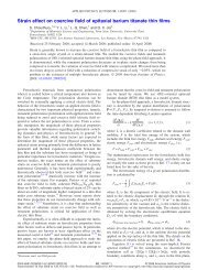
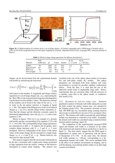
(a)<br />
d 3<br />
Q 1<br />
Q 2<br />
Q 3<br />
V Q<br />
(b)<br />
(c)<br />
0.8 µm<br />
Piezoresponse, a.u.<br />
4<br />
3<br />
2<br />
1<br />
0<br />
-1<br />
-2<br />
(d)<br />
s<strong>in</strong>gle data set<br />
one charge model<br />
0 1000 2000 3000 4000 5000<br />
Distance, nm<br />
Figure 19. (a) Representation of a realistic tip by a set of image charges. (b) Surface topography and (c) PFM image of doma<strong>in</strong> wall <strong>in</strong><br />
LNO. (d) Fit of the extrapolated data set with equal weight<strong>in</strong>g for all po<strong>in</strong>ts. Reproduced from [218]. Copyright 2007, American Institute of<br />
Physics.<br />
Table 2. Effective image charge parameters for different <strong>ferroelectric</strong>s.<br />
Wall R 0 for R 0 for<br />
Material width (nm) Q d (nm) R d (nm) ε e = 1(µm) ε e = 80 (nm)<br />
LiNbO 3 96 1000 92 58.6 4.8 60<br />
Epitaxial PZT 107 2550 125 79.6 5 62.5<br />
PZT <strong>in</strong> air 58 723 86.5 55.1 44 541<br />
PZT <strong>in</strong> liquid 6 104 11.8 7.5 75<br />
charges can be deconvoluted from the experimental doma<strong>in</strong><br />
wall profile by m<strong>in</strong>imiz<strong>in</strong>g the functional<br />
∫ ( 1<br />
F [u 3 ] = PR(a) −<br />
2πε 0 (ε e + κ)<br />
N∑<br />
m=0<br />
) 2<br />
Q m<br />
ũ 3 (s m ) da<br />
d m<br />
(2.29)<br />
with respect to the number, N, magnitude and charge–surface<br />
separation of a set of image charges {Q i ,d i } N represent<strong>in</strong>g the<br />
tip. Here PR(a) is the measured piezoresponse and <strong>in</strong>tegration<br />
is performed over all available a values. The dielectric constant<br />
of the medium can be fixed to the value of free air (ε e = 1)<br />
or water <strong>in</strong> the tip–surface junction or imag<strong>in</strong>g <strong>in</strong> liquid<br />
(ε e = 80). The output of the fitt<strong>in</strong>g process is the set of reduced<br />
charges q i = Q i /2πε 0 and the charge surface separation, d i .<br />
Note that the charges and the dielectric constants cannot be<br />
determ<strong>in</strong>ed <strong>in</strong>dependently, s<strong>in</strong>ce only Q m /(ε e + κ)ratios enter<br />
equation (2.29).<br />
Shown <strong>in</strong> figures 19(b)–(d) is an example of a doma<strong>in</strong><br />
wall profile and the correspond<strong>in</strong>g fit by equation (2.29) with<br />
N = 1 for LNO. The correspond<strong>in</strong>g image charge parameters<br />
are summarized <strong>in</strong> table 2. To improve the fit quality, more<br />
complex fitt<strong>in</strong>g functions with N = 2 and N = 3 were<br />
attempted. However, <strong>in</strong>dependent of the choice of the <strong>in</strong>itial<br />
values of the image charge, the fit converged to a s<strong>in</strong>gle image<br />
charge, i.e. d i = d and ∑ Q i = Q. Similar behavior was<br />
observed for other doma<strong>in</strong> walls.<br />
This analysis suggests that the electrostatic field produced<br />
by the tip is consistent with a s<strong>in</strong>gle po<strong>in</strong>t charge positioned<br />
at large separation from the surface, contrary to the behavior<br />
anticipated <strong>in</strong> contact mode imag<strong>in</strong>g. The analysis was<br />
extended to the case of the sphere–plane (radius of curvature<br />
R 0 ) and disk–plane (radius R d ) models. The sphere<br />
parameters are calculated both from ambient and water<br />
environment to account for possible capillary condensation<br />
effects. From the data, it is clear that the use of the<br />
sphere/air model leads to implausibly large radii. Hence,<br />
experimental data are consistent either with the presence of<br />
a capillary water film <strong>in</strong> the sphere model, or conductive<br />
disk model [218].<br />
2.4.2. Resolution for non-zero contact area. Extensive<br />
quantitative analysis of doma<strong>in</strong> wall width, tak<strong>in</strong>g <strong>in</strong>to account<br />
the f<strong>in</strong>ite contact tip–surface contact area, was reported by<br />
the Gopalan group [183]. The geometric structure of more<br />
than 100 SPM tips was ascerta<strong>in</strong>ed us<strong>in</strong>g scann<strong>in</strong>g electron<br />
microscopy to yield effective tip sizes [212], see figures 20(a)<br />
and (b). The doma<strong>in</strong> wall width <strong>in</strong> periodically poled lithium<br />
niobate was measured as a function of tip radius. In parallel,<br />
the doma<strong>in</strong> wall width was calculated us<strong>in</strong>g a numerical f<strong>in</strong>ite<br />
element analysis package, figure 20.<br />
The comparison of the experimentally measured PFM<br />
signal and doma<strong>in</strong> wall width as a function of tip radius<br />
with numerical and analytical theory predictions is shown <strong>in</strong><br />
figure 21. The data clearly suggest that the PFM signal is<br />
<strong>in</strong>dependent of contact area, <strong>in</strong> agreement with the theory<br />
of Karapetian [175, 176]. At the same time, the doma<strong>in</strong><br />
wall width saturates at ∼100 nm, correspond<strong>in</strong>g to a tip<strong>in</strong>dependent<br />
doma<strong>in</strong> wall width. This can be attributed both<br />
to the effect of an ambient environment on imag<strong>in</strong>g, and to<br />
wall broaden<strong>in</strong>g, necessitat<strong>in</strong>g further studies <strong>in</strong> an ultra-high<br />
vacuum environment.<br />
21