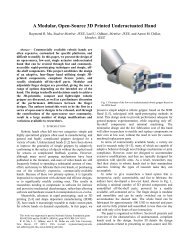
Noncontact Atomic Force Microscopy - Yale School of Engineering ...
Noncontact Atomic Force Microscopy - Yale School of Engineering ...
Noncontact Atomic Force Microscopy - Yale School of Engineering ...

Create successful ePaper yourself
Turn your PDF publications into a flip-book with our unique Google optimized e-Paper software.
P.I-09<br />
Contact potential difference on the atomic-scale probed by<br />
Kelvin Probe <strong>Force</strong> <strong>Microscopy</strong>: an imaging scenario<br />
Laurent Nony 1 , Adam Foster 2 , Franck Bocquet 1 , and Christian Loppacher 1<br />
1<br />
Aix-Marseille Université, IM2NP, Av. Escadrille Normandie-Niemen, F-13397 Marseille and CNRS, IM2NP (UMR<br />
6242), Marseille-Toulon, France<br />
2<br />
Department <strong>of</strong> Physics, Tampere University <strong>of</strong> Technology,<br />
P.O. Box 692 FIN-33101 Tampere, Finland<br />
A fully numerical analysis <strong>of</strong> the origin <strong>of</strong> the atomic-scale contrast in Kelvin probe force<br />
microscopy (KPFM) is presented. The numerical implementation mimics recent experimental<br />
results on the (001) surface <strong>of</strong> a bulk alkali halide single crystal for which a simultaneous<br />
topographical and Kelvin, so-called Contact Potential Difference (CPD), atomic-scale contrast<br />
had been reported [1]. In this work, we have combined atomistic simulations <strong>of</strong> the tip-sample<br />
force field with our non-contact AFM/KPFM simulator [2] to compute topographical and CPD<br />
images. The force field notably includes the required short-range bias voltage dependence to<br />
account for the CPD atomic-scale contrast. The sample is a NaCl(001) single crystal. The<br />
atomistic simulations have been performed by means <strong>of</strong> the code SCIFI [3]. The simulator has<br />
been used in the Frequency-Modulation KPFM operating mode. The tip consists <strong>of</strong> a spherical<br />
metallic cap within which a 4x4x4 NaCl cluster with the [111] direction pointing towards the<br />
surface is partly embedded. The sample consists <strong>of</strong> a 10x10x4 NaCl slab embedded within a<br />
semi-infinite continuous medium merely described by its dielectric constant. The sample, with a<br />
macroscopic height (several millimeters), lies on a metallic counter-electrode that is biased with<br />
respect to the tip. Beyond the short-range chemical and electrostatic forces computed with SCIFI,<br />
we have included a usual Van der Waals long-range term and a less usual, although fundamental,<br />
long-range electrostatic interaction. This term mimics the weak capacitive interaction between tip<br />
and sample holders and is necessary to describe the behavior <strong>of</strong> the CPD with the distance.<br />
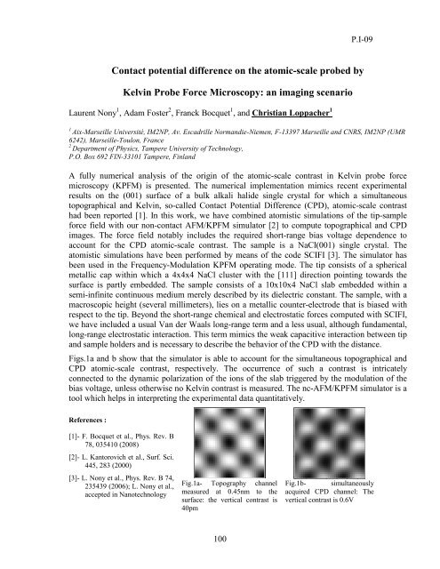
Figs.1a and b show that the simulator is able to account for the simultaneous topographical and<br />
CPD atomic-scale contrast, respectively. The occurrence <strong>of</strong> such a contrast is intricately<br />
connected to the dynamic polarization <strong>of</strong> the ions <strong>of</strong> the slab triggered by the modulation <strong>of</strong> the<br />
bias voltage, unless otherwise no Kelvin contrast is measured. The nc-AFM/KPFM simulator is a<br />
tool which helps in interpreting the experimental data quantitatively.<br />
References :<br />
[1]- F. Bocquet et al., Phys. Rev. B<br />
78, 035410 (2008)<br />
[2]- L. Kantorovich et al., Surf. Sci.<br />
445, 283 (2000)<br />
[3]- L. Nony et al., Phys. Rev. B 74,<br />
235439 (2006); L. Nony et al.,<br />
accepted in Nanotechnology<br />
Fig.1a- Topography channel<br />
measured at 0.45nm to the<br />
surface: the vertical contrast is<br />
40pm<br />
100<br />
Fig.1b- simultaneously<br />
acquired CPD channel: The<br />
vertical contrast is 0.6V