Noncontact Atomic Force Microscopy - Yale School of Engineering ...
Noncontact Atomic Force Microscopy - Yale School of Engineering ...
Noncontact Atomic Force Microscopy - Yale School of Engineering ...

You also want an ePaper? Increase the reach of your titles
YUMPU automatically turns print PDFs into web optimized ePapers that Google loves.
P.II-30<br />
Probing Local Bias-Induced Phase Transitions on the Single Defect<br />
Level: from Imaging to Deterministic Mechanisms<br />
N. Balke 1 , S. Jesse 1 , P. Maksymovych 1 , Y.H. Chu 2 , R. Ramesh 2 , S. Choudhury 3 , L.Q.<br />
Chen 3 , and S.V. Kalinin 1<br />
1 Oak Ridge National Laboratory, Oak Ridge, TN 37831<br />
2 Dept. <strong>of</strong> Physics and Dept. <strong>of</strong> Mat. Sci. and Eng., University <strong>of</strong> California, Berkeley, CA<br />
3 Dept. <strong>of</strong> Mat. Sci. and Eng., Pennsylvania State University, University Park, PA 16802<br />
<strong>Force</strong>-induced processes such a molecular unfolding spectroscopy and NC-AFM<br />
atomic manipulation now underpin many areas <strong>of</strong> physics and biology. Here, I discuss<br />
recent progress on probing local bias-induced phase transitions in ferroelectrics and<br />
electrochemical systems. Bias-induced phase transitions are controlled by structural<br />
defects that act both as the local nucleation centers and the pinning centers for moving<br />
domain walls. Future progress necessitates understanding <strong>of</strong> polarization switching<br />
mechanisms on the single structural or morphological defect level. In this talk, I will<br />
present results on local studies <strong>of</strong> polarization reversal mechanisms in ferroelectrics [1-2].<br />
The direct imaging <strong>of</strong> a single nucleation center on the sub-100 nanometer level is<br />
demonstrated [3]. By using switching spectroscopy Piezoresponse <strong>Force</strong> <strong>Microscopy</strong> on<br />
systems with engineered defect structures and phase-field modeling, we demonstrate that<br />
deterministic that mesoscopic polarization switching mechanisms on single 1D and 2D<br />
defects can be determined. We develop a framework to link the modeling results to<br />
experimental observations using neural-network based recognition. The future potential<br />
for atomistic studies is discussed. Research was supported by the U.S. Department <strong>of</strong><br />
Energy Office <strong>of</strong> Basic Energy Sciences Division <strong>of</strong> Scientific User Instruments and was<br />
performed at Oak Ridge National Laboratory which is operated by UT-Battelle, LLC.<br />
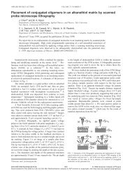
Figure 1: (a) Surface topography and (b) SS-PFM nucleation bias map <strong>of</strong> BiFeO3 24deg (100)<br />
bicrystal grain boundary (GB). Each point in (b) is a hysteresis loop. (c) Ferroelectric switching<br />
properties across the interface.<br />
[1] S.V. Kalinin, B.J. Rodriguez, S. Jesse, Y.H. Chu, T. Zhao, R. Ramesh, E.A. Eliseev, and A.N.<br />
Morozovska, PNAS 104, 20204 (2007).<br />
[2] S. Jesse, B.J. Rodriguez, A.P. Baddorf, I. Vrejoiu, D. Hesse, M. Alexe, E.A. Eliseev, A.N. Morozovska,<br />
and S.V. Kalinin, Nature Materials 7, 209 (2008).<br />
[3] S.V. Kalinin, S. Jesse, B.J. Rodriguez, Y.H. Chu, R. Ramesh, E.A. Eliseev and A.N. Morozovska, Phys.<br />
Rev. Lett. 100, 155703 (2008)<br />
158