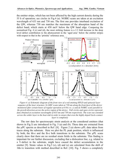
- Page 1 and 2:
AdvancesinOptics,Photonics,Spectros
- Page 3 and 4:
Những tiến bộ trongQuang họ
- Page 5 and 6:
KỶ YẾU CÁC HỘI NGHỊo Hội
- Page 7 and 8:
MỤC LỤCThông tin về hội ng
- Page 9 and 10:
NATURAL RADIOACTIVITY IN SOME ANCIE
- Page 12 and 13:
THIẾT KẾ VÀ CHẾ TẠO CHIP C
- Page 14 and 15:
HỌC CHƯƠNG TRÌNH VẬT LÝ THP
- Page 16 and 17:
Conference TopicsQuantum PhotonicsP
- Page 18 and 19:
Invited speakersNguyen Van Hieu (VA
- Page 20 and 21:
SESSION A1: QUANTUM PHOTONICS AND N
- Page 22 and 23:
Chairperson: Dr. Phan Ngoc Minh (IM
- Page 24 and 25:
SESSION A2 :SPECTROSCOPY OF CONDENS
- Page 26:
(A2-14)08: 45 - 09: 05 FABRICATION,
- Page 29 and 30:
(A2-36)09: 00 - 09: 20 NANO PARTICA
- Page 31 and 32:
SESSION B: OPTICS, LASERS and PHOTO
- Page 33 and 34:
(B-13)08: 45 - 09: 05 FREQUENCY STA
- Page 35 and 36:
(B-27)16: 30 - 16: 50 DEVERLOPMENT
- Page 37 and 38:
14: 10 - 14: 30 THE SEMI-STATISTICA
- Page 39 and 40:
(C-07)10: 15 - 10: 35 THERMOLUMINES
- Page 41 and 42:
(C-22)08: 30 - 08: 50 DESIGN AND FA
- Page 43:
(C-37)15: 30 - 15: 50 CACULATING EM
- Page 46 and 47:
___________________________________
- Page 48 and 49:
___________________________________
- Page 50 and 51:
___________________________________
- Page 52 and 53:
___________________________________
- Page 54 and 55:
___________________________________
- Page 56 and 57:
___________________________________
- Page 58 and 59:
___________________________________
- Page 60 and 61:
___________________________________
- Page 62 and 63:
___________________________________
- Page 64 and 65:
___________________________________
- Page 66 and 67:
___________________________________
- Page 68 and 69:
___________________________________
- Page 70 and 71:
___________________________________
- Page 72 and 73:
___________________________________
- Page 74 and 75:
___________________________________
- Page 76 and 77:
___________________________________
- Page 78 and 79:
___________________________________
- Page 80 and 81:
___________________________________
- Page 82 and 83:
___________________________________
- Page 84 and 85:
___________________________________
- Page 86 and 87:
___________________________________
- Page 88 and 89:
___________________________________
- Page 90 and 91:
___________________________________
- Page 92 and 93:
___________________________________
- Page 94 and 95:
___________________________________
- Page 96 and 97:
___________________________________
- Page 98 and 99:
Intensity__________________________
- Page 100 and 101:
___________________________________
- Page 102 and 103:
___________________________________
- Page 104 and 105:
___________________________________
- Page 106 and 107:
___________________________________
- Page 108 and 109:
XRD intensity (arb. units)_________
- Page 110 and 111:
___________________________________
- Page 112 and 113:
mat do dong(mA)____________________
- Page 114 and 115:
___________________________________
- Page 116 and 117:
___________________________________
- Page 118 and 119:
___________________________________
- Page 120 and 121:
Target Substrate Distance 40mmNumbe
- Page 122 and 123:
___________________________________
- Page 124 and 125:
___________________________________
- Page 126 and 127:
___________________________________
- Page 128 and 129:
___________________________________
- Page 130 and 131:
mGy________________________________
- Page 132 and 133:
___________________________________
- Page 134 and 135:
___________________________________
- Page 136 and 137:
___________________________________
- Page 138 and 139:
___________________________________
- Page 140 and 141:
___________________________________
- Page 142 and 143:
___________________________________
- Page 144 and 145:
___________________________________
- Page 146 and 147:
I TL(a.u.)I TL(a.u.)I TL(a.u.)_____
- Page 148 and 149:
___________________________________
- Page 150 and 151:
___________________________________
- Page 152 and 153:
___________________________________
- Page 154 and 155:
___________________________________
- Page 156 and 157:
Counts_____________________________
- Page 158 and 159:
___________________________________
- Page 160 and 161:
___________________________________
- Page 162 and 163:
Intensity__________________________
- Page 164 and 165:
___________________________________
- Page 166 and 167:
___________________________________
- Page 168 and 169:
___________________________________
- Page 170 and 171:
___________________________________
- Page 172 and 173:
___________________________________
- Page 174 and 175:
___________________________________
- Page 176 and 177:
___________________________________
- Page 178 and 179:
Intensity (arb. units)_____________
- Page 180 and 181:
Intensity (counts/s)_______________
- Page 182 and 183:
___________________________________
- Page 184 and 185:
M(emu/g)___________________________
- Page 186 and 187:
___________________________________
- Page 188 and 189:
___________________________________
- Page 190 and 191:
___________________________________
- Page 192 and 193:
___________________________________
- Page 194 and 195:
___________________________________
- Page 196 and 197:
___________________________________
- Page 198 and 199:
___________________________________
- Page 200 and 201:
___________________________________
- Page 202 and 203:
___________________________________
- Page 204 and 205:
___________________________________
- Page 206 and 207:
___________________________________
- Page 208 and 209:
___________________________________
- Page 210 and 211:
___________________________________
- Page 212 and 213:
Cêng ®é TL (®vt®)___________
- Page 214 and 215:
___________________________________
- Page 216 and 217:
___________________________________
- Page 218 and 219:
___________________________________
- Page 220 and 221:
___________________________________
- Page 222 and 223:
___________________________________
- Page 224 and 225:
___________________________________
- Page 226 and 227:
___________________________________
- Page 228 and 229:
___________________________________
- Page 230 and 231:
___________________________________
- Page 232 and 233:
___________________________________
- Page 234 and 235:
___________________________________
- Page 236 and 237:
___________________________________
- Page 238 and 239:
___________________________________
- Page 240 and 241:
___________________________________
- Page 242 and 243:
___________________________________
- Page 244 and 245:
___________________________________
- Page 246 and 247:
___________________________________
- Page 248 and 249:
___________________________________
- Page 250 and 251: ___________________________________
- Page 252 and 253: ___________________________________
- Page 254 and 255: ___________________________________
- Page 256 and 257: ___________________________________
- Page 258 and 259: ___________________________________
- Page 260 and 261: ___________________________________
- Page 262 and 263: ___________________________________
- Page 264 and 265: ___________________________________
- Page 266 and 267: ___________________________________
- Page 268 and 269: ___________________________________
- Page 270 and 271: C«ng suÊt quang ra, mWC«ng suÊt
- Page 272 and 273: ___________________________________
- Page 274 and 275: ___________________________________
- Page 276 and 277: ___________________________________
- Page 278 and 279: ___________________________________
- Page 280 and 281: ___________________________________
- Page 282 and 283: ___________________________________
- Page 284 and 285: ___________________________________
- Page 286 and 287: ___________________________________
- Page 288 and 289: ___________________________________
- Page 290 and 291: Những tiến bộ trong Quang h
- Page 292 and 293: ___________________________________
- Page 294 and 295: ___________________________________
- Page 296 and 297: 3.4 Reliability of resultsFigure 1
- Page 298 and 299: ___________________________________
- Page 302 and 303: ___________________________________
- Page 304 and 305: ___________________________________
- Page 306 and 307: ___________________________________
- Page 308 and 309: ___________________________________
- Page 310 and 311: Những tiến bộ trong Quang h
- Page 312 and 313: Những tiến bộ trong Quang h
- Page 314 and 315: Những tiến bộ trong Quang h
- Page 316 and 317: ___________________________________
- Page 318 and 319: ___________________________________
- Page 320 and 321: ___________________________________
- Page 322 and 323: ___________________________________
- Page 324 and 325: ___________________________________
- Page 326 and 327: ___________________________________
- Page 328 and 329: ___________________________________
- Page 330 and 331: Cêng ®é (®¬n vÞ tuú ý)___
- Page 332 and 333: ___________________________________
- Page 334 and 335: ___________________________________
- Page 336 and 337: ___________________________________
- Page 338 and 339: ___________________________________
- Page 340 and 341: ___________________________________
- Page 342 and 343: ___________________________________
- Page 344 and 345: ___________________________________
- Page 346 and 347: ___________________________________
- Page 348 and 349: ốđin g__________________________
- Page 350 and 351:
___________________________________
- Page 352 and 353:
___________________________________
- Page 354 and 355:
___________________________________
- Page 356 and 357:
___________________________________
- Page 358 and 359:
___________________________________
- Page 360 and 361:
___________________________________
- Page 362 and 363:
___________________________________
- Page 364 and 365:
___________________________________
- Page 366 and 367:
___________________________________
- Page 368 and 369:
___________________________________
- Page 370 and 371:
___________________________________
- Page 372 and 373:
___________________________________
- Page 374 and 375:
___________________________________
- Page 376 and 377:
___________________________________
- Page 378 and 379:
___________________________________
- Page 380 and 381:
___________________________________
- Page 382 and 383:
___________________________________
- Page 384 and 385:
___________________________________
- Page 386 and 387:
___________________________________
- Page 388 and 389:
___________________________________
- Page 390 and 391:
___________________________________
- Page 392 and 393:
___________________________________
- Page 394 and 395:
Abs (S)____________________________
- Page 396 and 397:
___________________________________
- Page 398 and 399:
TransmittanceReflectance___________
- Page 400 and 401:
___________________________________
- Page 402 and 403:
§¸p øng liÒu Gamma (counts)§¸
- Page 404 and 405:
Excitation(nm)Excitation(nm)_______
- Page 406 and 407:
___________________________________
- Page 408 and 409:
___________________________________
- Page 410 and 411:
Cêng ®é TL (®vt®)Cêng ®
- Page 412 and 413:
___________________________________
- Page 414 and 415:
___________________________________
- Page 416 and 417:
___________________________________
- Page 418 and 419:
___________________________________
- Page 420 and 421:
___________________________________
- Page 422 and 423:
___________________________________
- Page 424 and 425:
___________________________________
- Page 426 and 427:
___________________________________
- Page 428 and 429:
___________________________________
- Page 430 and 431:
___________________________________
- Page 432 and 433:
___________________________________
- Page 434 and 435:
___________________________________
- Page 436 and 437:
Những tiến bộ trong Quang h
- Page 438 and 439:
Những tiến bộ trong Quang h
- Page 440 and 441:
Những tiến bộ trong Quang h
- Page 442 and 443:
___________________________________
- Page 444 and 445:
___________________________________
- Page 446 and 447:
___________________________________
- Page 448 and 449:
___________________________________
- Page 450 and 451:
___________________________________
- Page 452 and 453:
___________________________________
- Page 454 and 455:
___________________________________
- Page 456 and 457:
___________________________________
- Page 458 and 459:
___________________________________
- Page 460 and 461:
___________________________________
- Page 462 and 463:
___________________________________
- Page 464 and 465:
___________________________________
- Page 466 and 467:
___________________________________
- Page 468 and 469:
___________________________________
- Page 470 and 471:
___________________________________
- Page 472 and 473:
X 2 (m)____________________________
- Page 474 and 475:
___________________________________
- Page 476 and 477:
___________________________________
- Page 478 and 479:
___________________________________
- Page 480 and 481:
___________________________________
- Page 482 and 483:
___________________________________
- Page 484 and 485:
___________________________________
- Page 486 and 487:
___________________________________
- Page 488 and 489:
___________________________________
- Page 490 and 491:
___________________________________
- Page 492 and 493:
___________________________________
- Page 494 and 495:
___________________________________
- Page 496 and 497:
___________________________________
- Page 498 and 499:
___________________________________
- Page 500 and 501:
___________________________________
- Page 502 and 503:
___________________________________
- Page 504 and 505:
___________________________________
- Page 506 and 507:
___________________________________
- Page 508 and 509:
___________________________________
- Page 510 and 511:
___________________________________
- Page 512 and 513:
___________________________________
- Page 514 and 515:
___________________________________
- Page 516 and 517:
___________________________________
- Page 518 and 519:
___________________________________
- Page 520 and 521:
___________________________________
- Page 522 and 523:
___________________________________
- Page 524 and 525:
C«ng suÊt ph¸t [W]______________
- Page 526 and 527:
___________________________________
- Page 528 and 529:
___________________________________
- Page 530 and 531:
C«ng suÊt (W)____________________
- Page 532 and 533:
___________________________________
- Page 534 and 535:
Transmission (%)External Transmissi
- Page 536 and 537:
___________________________________
- Page 538 and 539:
___________________________________
- Page 540 and 541:
___________________________________
- Page 542 and 543:
___________________________________
- Page 544 and 545:
___________________________________
- Page 546 and 547:
___________________________________
- Page 548 and 549:
___________________________________
- Page 550 and 551:
___________________________________
- Page 552 and 553:
___________________________________
- Page 554 and 555:
___________________________________
- Page 556 and 557:
___________________________________
- Page 558 and 559:
___________________________________
- Page 560 and 561:
DANH SÁCH CÁC BÀI ĐƯỢC ĐĂN
- Page 562:
Le Dinh Trong, Pham Duy Long, Vu Va