- Page 1 and 2: Materials for engineering Third edi
- Page 3 and 4: Related titles: Solving tribology p
- Page 5 and 6: Woodhead Publishing Limited and Man
- Page 7 and 8: vi Contents 3.4 Degradation of meta
- Page 10: Preface to the third edition The cr
- Page 14: Preface to the first edition This t
- Page 17 and 18: xvi Introduction Young’s modulus,
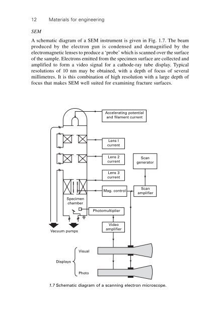
- Page 20 and 21: 1 Structure of engineering material
- Page 22 and 23: Structure of engineering materials
- Page 24 and 25: 1.2 Microstructure Structure of eng
- Page 26 and 27: Structure of engineering materials
- Page 30 and 31: Structure of engineering materials
- Page 32 and 33: Structure of engineering materials
- Page 34 and 35: Structure of engineering materials
- Page 36 and 37: Structure of engineering materials
- Page 38 and 39: Structure of engineering materials
- Page 40 and 41: Structure of engineering materials
- Page 42 and 43: Structure of engineering materials
- Page 44 and 45: Structure of engineering materials
- Page 46 and 47: Structure of engineering materials
- Page 48 and 49: Structure of engineering materials
- Page 50 and 51: Structure of engineering materials
- Page 52: 1.4 Further reading Structure of en
- Page 55 and 56: 38 Materials for engineering Stress
- Page 57 and 58: 40 Materials for engineering The BE
- Page 59 and 60: 42 Materials for engineering presen
- Page 61 and 62: 44 Materials for engineering the ca
- Page 63 and 64: 46 Materials for engineering 2.5.2
- Page 65 and 66: 48 Materials for engineering tough
- Page 67 and 68: 50 Materials for engineering d/dc (
- Page 69 and 70: 52 Materials for engineering releas
- Page 71 and 72: 54 Materials for engineering a know
- Page 73 and 74: 56 Materials for engineering Figure
- Page 75 and 76: 58 Materials for engineering σ a
- Page 77 and 78: 60 Materials for engineering 10 -2
- Page 79 and 80:
62 Materials for engineering 10 4 E
- Page 81 and 82:
64 Materials for engineering III a
- Page 83 and 84:
66 Materials for engineering (a) (b
- Page 86:
Part II Structure-property relation
- Page 89 and 90:
72 Materials for engineering where
- Page 91 and 92:
74 Materials for engineering 815 Te
- Page 93 and 94:
76 Materials for engineering the te
- Page 95 and 96:
78 Materials for engineering ageing
- Page 97 and 98:
80 Materials for engineering behavi
- Page 99 and 100:
82 Materials for engineering creep
- Page 101 and 102:
84 Materials for engineering an imp
- Page 103 and 104:
86 Materials for engineering Alumin
- Page 105 and 106:
88 Materials for engineering Duralu
- Page 107 and 108:
90 Materials for engineering Weight
- Page 109 and 110:
92 Materials for engineering β α
- Page 111 and 112:
94 Materials for engineering RT = r
- Page 113 and 114:
96 Materials for engineering 1400 1
- Page 115 and 116:
98 Materials for engineering Tensil
- Page 117 and 118:
100 Materials for engineering At% A
- Page 119 and 120:
102 Materials for engineering to th
- Page 121 and 122:
104 Materials for engineering 1600
- Page 123 and 124:
106 Materials for engineering Heat-
- Page 125 and 126:
108 Materials for engineering The p
- Page 127 and 128:
110 Materials for engineering featu
- Page 129 and 130:
112 Materials for engineering pheno
- Page 131 and 132:
114 Materials for engineering Tensi
- Page 133 and 134:
116 Materials for engineering 3.3.2
- Page 135 and 136:
118 Materials for engineering and c
- Page 137 and 138:
120 Materials for engineering is sm
- Page 139 and 140:
122 Materials for engineering polyb
- Page 141 and 142:
124 Materials for engineering crack
- Page 143 and 144:
126 Materials for engineering the l
- Page 145 and 146:
128 Materials for engineering initi
- Page 147 and 148:
130 Materials for engineering Wear
- Page 149 and 150:
132 Materials for engineering I.J.
- Page 151 and 152:
134 Materials for engineering Na -
- Page 153 and 154:
136 Materials for engineering where
- Page 155 and 156:
138 Materials for engineering 4.1.5
- Page 157 and 158:
140 Materials for engineering such
- Page 159 and 160:
142 Materials for engineering Table
- Page 161 and 162:
144 Materials for engineering O 2-
- Page 163 and 164:
146 Materials for engineering resis
- Page 165 and 166:
148 Materials for engineering 55% t
- Page 167 and 168:
150 Materials for engineering to-ge
- Page 169 and 170:
152 Materials for engineering large
- Page 171 and 172:
154 Materials for engineering Up to
- Page 173 and 174:
156 Materials for engineering stres
- Page 175 and 176:
158 Materials for engineering 2500
- Page 177 and 178:
160 Materials for engineering Amorp
- Page 179 and 180:
162 Materials for engineering screw
- Page 181 and 182:
164 Materials for engineering 2 3 4
- Page 183 and 184:
166 Materials for engineering 5.4.2
- Page 185 and 186:
168 Materials for engineering Tough
- Page 187 and 188:
170 Materials for engineering Craze
- Page 189 and 190:
172 Materials for engineering 10 Te
- Page 191 and 192:
174 Materials for engineering by a
- Page 193 and 194:
176 Materials for engineering 10 -1
- Page 195 and 196:
178 Materials for engineering the t
- Page 197 and 198:
180 Materials for engineering energ
- Page 199 and 200:
182 Materials for engineering 30 4.
- Page 201 and 202:
184 Materials for engineering Atomi
- Page 203 and 204:
186 Materials for engineering 6.2 M
- Page 205 and 206:
188 Materials for engineering limes
- Page 207 and 208:
190 Materials for engineering 6-20%
- Page 209 and 210:
192 Materials for engineering Table
- Page 211 and 212:
194 Materials for engineering runs
- Page 213 and 214:
196 Materials for engineering where
- Page 215 and 216:
198 Materials for engineering agree
- Page 217 and 218:
200 Materials for engineering 100 S
- Page 219 and 220:
202 Materials for engineering 6.4.2
- Page 221 and 222:
204 Materials for engineering σ f
- Page 223 and 224:
206 Materials for engineering d = 2
- Page 225 and 226:
208 Materials for engineering A fib
- Page 227 and 228:
210 Materials for engineering But l
- Page 229 and 230:
212 Materials for engineering 10 -3
- Page 231 and 232:
214 Materials for engineering envir
- Page 234:
Part III Problems
- Page 237 and 238:
220 Materials for engineering Liqui
- Page 239 and 240:
222 Materials for engineering 3. Eq
- Page 241 and 242:
224 Materials for engineering to a
- Page 243 and 244:
226 Materials for engineering Chapt
- Page 245 and 246:
228 Materials for engineering carbi
- Page 248:
Appendix I Useful constants Symbol
- Page 251 and 252:
234 Appendix II Fracture toughness
- Page 254 and 255:
Appendix IV Sources of material pro
- Page 256:
Sources of material property data 2
- Page 260 and 261:
Index acrylics 160 adhesives 121 ad
- Page 262 and 263:
Index 245 smart fibre 189 stiffness
- Page 264 and 265:
Index 247 GPC (gel permeation chrom
- Page 266 and 267:
Index 249 offset yield strength 39
- Page 268 and 269:
Index 251 nitriding 83-4 normalisin