

TC1765_ds_v12 (TC1765_ds_v12_1202.pdf) - Infineon
TC1765_ds_v12 (TC1765_ds_v12_1202.pdf) - Infineon
TC1765_ds_v12 (TC1765_ds_v12_1202.pdf) - Infineon
- TAGS
- infineon
- www.infineon.com

You also want an ePaper? Increase the reach of your titles
YUMPU automatically turns print PDFs into web optimized ePapers that Google loves.
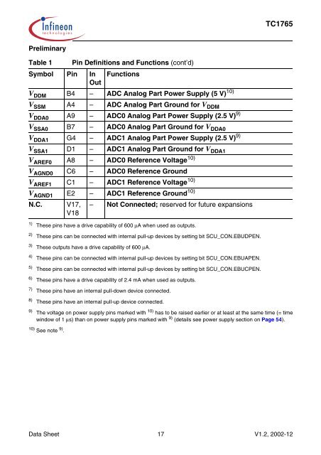
Preliminary<br />
Table 1 Pin Definitions and Functions (cont’d)<br />
Symbol Pin In<br />
Out<br />
Functions<br />
V DDM B4 – ADC Analog Part Power Supply (5 V) 10)<br />
V SSM A4 – ADC Analog Part Ground for V DDM<br />
V DDA0 A9 – ADC0 Analog Part Power Supply (2.5 V) 9)<br />
V SSA0 B7 – ADC0 Analog Part Ground for V DDA0<br />
V DDA1 G4 – ADC1 Analog Part Power Supply (2.5 V) 9)<br />
V SSA1 D1 – ADC1 Analog Part Ground for V DDA1<br />
V AREF0 A8 – ADC0 Reference Voltage 10)<br />
V AGND0 C6 – ADC0 Reference Ground<br />
V AREF1 C1 – ADC1 Reference Voltage 10)<br />
V AGND1 E2 – ADC1 Reference Ground 10)<br />
N.C. V17,<br />
V18<br />
– Not Connected; reserved for future expansions<br />
1) These pins have a drive capability of 600 µA when used as outputs.<br />
2) These pins can be connected with internal pull-up devices by setting bit SCU_CON.EBUDPEN.<br />
3) These outputs have a drive capability of 600 µA.<br />
4) These pins can be connected with internal pull-up devices by setting bit SCU_CON.EBUAPEN.<br />
5) These pins can be connected with internal pull-up devices by setting bit SCU_CON.EBUCPEN.<br />
6) These pins have a drive capability of 2.4 mA when used as outputs.<br />
7) These pins have an internal pull-down device connected.<br />
8) These pins have an internal pull-up device connected.<br />
<strong>TC1765</strong><br />
9) The voltage on power supply pins marked with 10) has to be raised earlier or at least at the same time (= time<br />
window of 1 µs) than on power supply pins marked with 9) (details see power supply section on Page 54).<br />
10) See note 9) .<br />
Data Sheet 17 V1.2, 2002-12


