

TC1765_ds_v12 (TC1765_ds_v12_1202.pdf) - Infineon
TC1765_ds_v12 (TC1765_ds_v12_1202.pdf) - Infineon
TC1765_ds_v12 (TC1765_ds_v12_1202.pdf) - Infineon
- TAGS
- infineon
- www.infineon.com

Create successful ePaper yourself
Turn your PDF publications into a flip-book with our unique Google optimized e-Paper software.
Preliminary<br />
<strong>TC1765</strong><br />
High-Speed Synchronous Serial Interfaces<br />
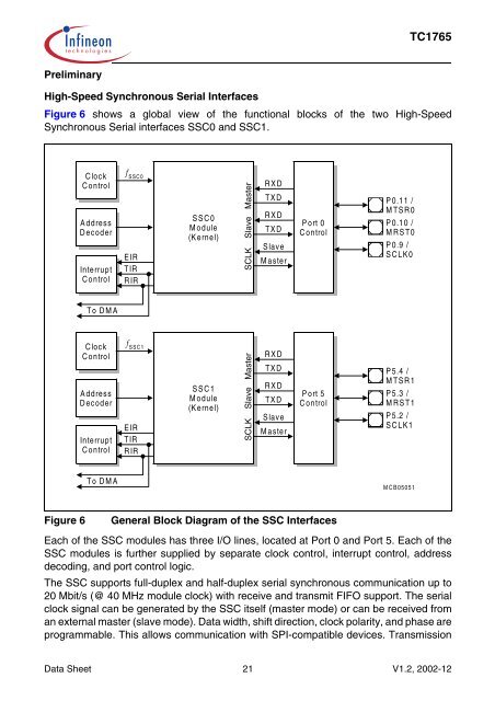
Figure 6 shows a global view of the functional blocks of the two High-Speed<br />
Synchronous Serial interfaces SSC0 and SSC1.<br />
Clock<br />
Control<br />
Address<br />
Decoder<br />
Interrupt<br />
Control<br />
To DMA<br />
Clock<br />
Control<br />
Address<br />
Decoder<br />
Interrupt<br />
Control<br />
To DMA<br />
f SSC0<br />
EIR<br />
TIR<br />
RIR<br />
f SSC1<br />
EIR<br />
TIR<br />
RIR<br />
SSC0<br />
Module<br />
(Kernel)<br />
SSC1<br />
Module<br />
(Kernel)<br />
Figure 6 General Block Diagram of the SSC Interfaces<br />
Master<br />
Slave<br />
SCLK<br />
Master<br />
Slave<br />
SCLK<br />
MCB05051<br />
Each of the SSC modules has three I/O lines, located at Port 0 and Port 5. Each of the<br />
SSC modules is further supplied by separate clock control, interrupt control, address<br />
decoding, and port control logic.<br />
The SSC supports full-duplex and half-duplex serial synchronous communication up to<br />
20 Mbit/s (@ 40 MHz module clock) with receive and transmit FIFO support. The serial<br />
clock signal can be generated by the SSC itself (master mode) or can be received from<br />
an external master (slave mode). Data width, shift direction, clock polarity, and phase are<br />
programmable. This allows communication with SPI-compatible devices. Transmission<br />
RXD<br />
TXD<br />
RXD<br />
TXD<br />
Slave<br />
Master<br />
RXD<br />
TXD<br />
RXD<br />
TXD<br />
Slave<br />
Master<br />
Port 0<br />
Control<br />
Port 5<br />
Control<br />
P0.11 /<br />
MTSR0<br />
P0.10 /<br />
MRST0<br />
P0.9 /<br />
SCLK0<br />
P5.4 /<br />
MTSR1<br />
P5.3 /<br />
MRST1<br />
P5.2 /<br />
SCLK1<br />
Data Sheet 21 V1.2, 2002-12


