

TC1765_ds_v12 (TC1765_ds_v12_1202.pdf) - Infineon
TC1765_ds_v12 (TC1765_ds_v12_1202.pdf) - Infineon
TC1765_ds_v12 (TC1765_ds_v12_1202.pdf) - Infineon
- TAGS
- infineon
- www.infineon.com

Create successful ePaper yourself
Turn your PDF publications into a flip-book with our unique Google optimized e-Paper software.
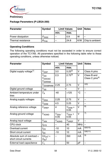
Preliminary<br />
Package Parameters (P-LBGA-260)<br />
Parameter Symbol Limit Values Unit Notes<br />
min. max.<br />
<strong>TC1765</strong><br />
Power dissipation PDISS – 0.9 W –<br />
Thermal resistance RTHA – 24.8 K/W Chip to ambient<br />
Operating Conditions<br />
The following operating conditions must not be exceeded in order to ensure correct<br />
operation of the <strong>TC1765</strong>. All parameters specified in the following table refer to these<br />
operating conditions, unless otherwise noticed.<br />
Parameter Symbol Limit Values Unit Notes<br />
min. max.<br />
Digital supply voltage 1) VDDP 3.0 5.25 2)<br />
V Class A pins<br />
VDD VDDOSC VDDRAM 2.3 2.75 3)<br />
V Class B and<br />
Class C pins 4)<br />
VDDSBRAM 2.25 2.75 V<br />
4)5)<br />
Digital ground voltage VSS 0 V –<br />
TA -40 +125 °C –<br />
Ambient temperature under<br />
bias<br />
Analog supply voltages VDDA 2.25 2.75 V –<br />
VDDM 4.5 5.25 V –<br />
Analog reference voltage V AREF 4 V DDM +<br />
0.05<br />
Analog ground voltage V AGND V SSA -<br />
0.05<br />
V SSA +<br />
0.05<br />
Analog input voltage V AIN V AGND V AREF V –<br />
CPU clock fSYS – 40 MHz –<br />
Overload current IOV -10 10 mA 8)9)10)<br />
Short circuit current ISC -10 10 mA 5)6)11)<br />
Absolute sum of overload +<br />
short circuit currents<br />
Σ|I OV| +<br />
|I SC|<br />
Data Sheet 58 V1.2, 2002-12<br />
V<br />
V<br />
6)<br />
7)<br />
– |50| mA 9)<br />
External load capacitance C L – 50 pF –


