

TC1765_ds_v12 (TC1765_ds_v12_1202.pdf) - Infineon
TC1765_ds_v12 (TC1765_ds_v12_1202.pdf) - Infineon
TC1765_ds_v12 (TC1765_ds_v12_1202.pdf) - Infineon
- TAGS
- infineon
- www.infineon.com

Create successful ePaper yourself
Turn your PDF publications into a flip-book with our unique Google optimized e-Paper software.
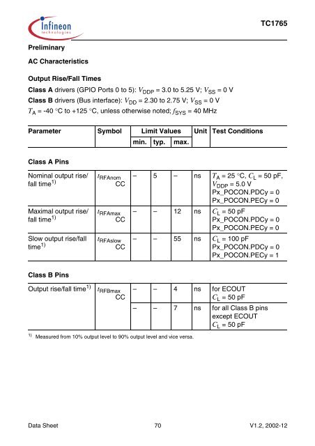
Preliminary<br />
AC Characteristics<br />
Output Rise/Fall Times<br />
Class A drivers (GPIO Ports 0 to 5): VDDP = 3.0 to 5.25 V; VSS = 0 V<br />
Class B drivers (Bus interface): VDD = 2.30 to 2.75 V; VSS = 0 V<br />
TA = -40 °C to +125 °C, unless otherwise noted; fSYS = 40 MHz<br />
Parameter Symbol Limit Values Unit Test Conditions<br />
min. typ. max.<br />
Class A Pins<br />
Nominal output rise/<br />
fall time 1)<br />
Maximal output rise/<br />
fall time 1)<br />
Slow output rise/fall<br />
time 1)<br />
Class B Pins<br />
t RFAnom<br />
CC<br />
t RFAmax<br />
CC<br />
t RFAslow<br />
CC<br />
Output rise/fall time 1) t RFBmax<br />
CC<br />
1) Measured from 10% output level to 90% output level and vice versa.<br />
<strong>TC1765</strong><br />
– 5 – ns T A = 25 °C, C L = 50 pF,<br />
V DDP = 5.0 V<br />
Px_POCON.PDCy = 0<br />
Px_POCON.PECy = 0<br />
– – 12 ns C L = 50 pF<br />
Px_POCON.PDCy = 0<br />
Px_POCON.PECy = 0<br />
– – 55 ns C L = 100 pF<br />
Px_POCON.PDCy = 0<br />
Px_POCON.PECy = 1<br />
– – 4 ns for ECOUT<br />
CL = 50 pF<br />
– – 7 ns for all Class B pins<br />
except ECOUT<br />
CL = 50 pF<br />
Data Sheet 70 V1.2, 2002-12


