Der UMC 0.18 Design Flow am Beispiel eines PDA ... - Mpc.belwue.de
Der UMC 0.18 Design Flow am Beispiel eines PDA ... - Mpc.belwue.de
Der UMC 0.18 Design Flow am Beispiel eines PDA ... - Mpc.belwue.de

Erfolgreiche ePaper selbst erstellen
Machen Sie aus Ihren PDF Publikationen ein blätterbares Flipbook mit unserer einzigartigen Google optimierten e-Paper Software.
FPGA Implementation of a HOG-based<br />
Pe<strong>de</strong>strian Recognition System<br />
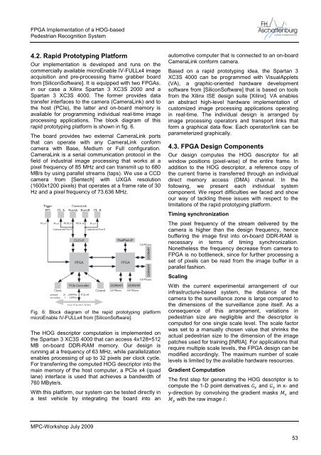
4.2. Rapid Prototyping Platform<br />
Our implementation is <strong>de</strong>veloped and runs on the<br />
commercially available microEnable IV-FULLx4 image<br />
acquisition and pre-processing fr<strong>am</strong>e grabber board<br />
from [SiliconSoftware]. It is equipped with two FPGAs,<br />
in our case a Xilinx Spartan 3 XC3S 2000 and a<br />
Spartan 3 XC3S 4000. The former provi<strong>de</strong>s data<br />
transfer interfaces to the c<strong>am</strong>era (C<strong>am</strong>eraLink) and to<br />
the host (PCIe), the latter and on-board memory is<br />
available for progr<strong>am</strong>ming individual real-time image<br />
processing applications. The block diagr<strong>am</strong> of this<br />
rapid prototyping platform is shown in fig. 6.<br />
The board provi<strong>de</strong>s two external C<strong>am</strong>eraLink ports<br />
that can operate with any C<strong>am</strong>eraLink conform<br />
c<strong>am</strong>era with Base, Medium or Full configuration.<br />
C<strong>am</strong>eraLink is a serial communication protocol in the<br />
field of industrial image processing that works at a<br />
pixel frequency of 85 MHz and can transmit up to 680<br />
MB/s by using parallel stre<strong>am</strong>s (taps). We use a CCD<br />
c<strong>am</strong>era from [Sentech] with UXGA resolution<br />
(1600x1200 pixels) that operates at a fr<strong>am</strong>e rate of 30<br />
Hz and a pixel frequency of 73.636 MHz.<br />
automotive computer that is connected to an on-board<br />
C<strong>am</strong>eraLink conform c<strong>am</strong>era.<br />
Based on a rapid prototyping i<strong>de</strong>a, the Spartan 3<br />
XC3S 4000 can be progr<strong>am</strong>med with VisualApplets<br />
(VA), a graphic-oriented hardware <strong>de</strong>velopment<br />
software from [SiliconSoftware] that is based on tools<br />
from the Xilinx ISE <strong>de</strong>sign suite [Xilinx]. VA enables<br />
an abstract high-level hardware implementation of<br />
customized image processing applications operating<br />
in real-time. The individual <strong>de</strong>sign is arranged by<br />
image processing operators and transport links that<br />
form a graphical data flow. Each operator/link can be<br />
par<strong>am</strong>eterized graphically.<br />
4.3. FPGA <strong>Design</strong> Components<br />
Our <strong>de</strong>sign computes the HOG <strong>de</strong>scriptor for all<br />
window positions (pixel-wise) of the entire fr<strong>am</strong>e. In<br />
addition to the HOG <strong>de</strong>scriptor, a reference copy of<br />
the current fr<strong>am</strong>e is transferred through an individual<br />
direct memory access (DMA) channel. In the<br />
following, we present each individual system<br />
component. We report difficulties we faced and show<br />
our way of tackling these issues with respect to the<br />
limitations of the rapid prototyping platform.<br />
Timing synchronization<br />
The pixel frequency of the stre<strong>am</strong> <strong>de</strong>livered by the<br />
c<strong>am</strong>era is higher than the <strong>de</strong>sign frequency, hence<br />
buffering the image first into on-board DDR-RAM is<br />
necessary in terms of timing synchronization.<br />
Nonetheless the frequency <strong>de</strong>crease from c<strong>am</strong>era to<br />
FPGA is no bottleneck, since for further processing a<br />
set of pixels can be read from the image buffer in a<br />
parallel fashion.<br />
Scaling<br />
Fig. 6: Block diagr<strong>am</strong> of the rapid prototyping platform<br />
microEnable IV-FULLx4 from [SiliconSoftware].<br />
The HOG <strong>de</strong>scriptor computation is implemented on<br />
the Spartan 3 XC3S 4000 that can access 4x128=512<br />
MB on-board DDR-RAM memory. Our <strong>de</strong>sign is<br />
running at a frequency of 63 MHz, while parallelization<br />
enables processing of up to 32 pixels per clock cycle.<br />
For transferring the computed HOG <strong>de</strong>scriptor into the<br />
main memory of the host computer, a PCIe x4 (quad<br />
lane) interface is used that achieves a bandwidth of<br />
760 MByte/s.<br />
With this platform, our system can be tested directly in<br />
a test vehicle by integrating the board into an<br />
With the current experimental arrangement of our<br />
infrastructure-based system, the distance of the<br />
c<strong>am</strong>era to the surveillance zone is large compared to<br />
the dimensions of the surveillance zone itself. As a<br />
consequence of this arrangement, variations in<br />
pe<strong>de</strong>strian size are negligible and the <strong>de</strong>scriptor is<br />
computed for one single scale level. The scale factor<br />
was set to a manually chosen value that shrinks the<br />
actual pe<strong>de</strong>strian size to the dimension of the image<br />
patches used for training [INRIA]. For applications that<br />
require multiple scale levels, the FPGA <strong>de</strong>sign can be<br />
modified accordingly. The maximum number of scale<br />
levels is limited by the available hardware resources.<br />
Gradient Computation<br />
The first step for generating the HOG <strong>de</strong>scriptor is to<br />
compute the 1-D point <strong>de</strong>rivatives and in x- and<br />
y-direction by convolving the gradient masks and<br />
with the raw image :<br />
MPC-Workshop July 2009<br />
53


![[Geben Sie hier die Überschrift ein] - MPC](https://img.yumpu.com/8654082/1/188x260/geben-sie-hier-die-uberschrift-ein-mpc.jpg?quality=85)