- Page 1 and 2:
MC9S12VR-Family Reference Manual S1
- Page 3 and 4:
Chapter 1 Device Overview MC9S12VR-
- Page 5 and 6:
Chapter 1 Device Overview MC9S12VR-
- Page 7 and 8:
2.3.34 Port L Analog Access Registe
- Page 9 and 10:
5.2 External Signal Description . .
- Page 11 and 12:
Chapter 9 Pulse-Width Modulator (S1
- Page 13 and 14:
12.4.6 Gated Time Accumulation Mode
- Page 15 and 16:
16.1.2 Modes of Operation . . . . .
- Page 17 and 18:
Appendix H LSDRV Electrical Specifi
- Page 19 and 20:
Chapter 1 Device Overview MC9S12VR-
- Page 21 and 22:
1.3 Chip-Level Features Feature MC9
- Page 23 and 24:
1.4.4 Main External Oscillator (XOS
- Page 25 and 26:
• Programmable polarity for trans
- Page 27 and 28:
1.5 Block Diagram PE0 PE1 VSUP VSS
- Page 29 and 30:
Address Module NOTE Reserved regist
- Page 31 and 32:
1.6.1 Part ID Assignments MC9S12VR
- Page 33 and 34:
1.7.2.7 PS[5:0] — Port S I/O Sign
- Page 35 and 36:
1.7.2.21 IOC[3:0] Signals MC9S12VR
- Page 37 and 38:
1.8.1 Pinout 48-pin LQFP LGND LIN (
- Page 39 and 40:
Package Function 48 LQ FP 32 LQ FP
- Page 41 and 42:
1.9 Modes of Operation MC9S12VR Fam
- Page 43 and 44:
1.11.2 Interrupt Vectors MC9S12VR F
- Page 45 and 46:
MC9S12VR Family Reference Manual, R
- Page 47 and 48:
Chapter 2 Port Integration Module (
- Page 49 and 50:
MC9S12VR Family Reference Manual, R
- Page 51 and 52:
Port Pin Name 2.3 Memory Map and Re
- Page 53 and 54:
Global Address 0x0243 Reserved 0x02
- Page 55 and 56:
Global Address 0x0272 Reserved 0x02
- Page 57 and 58:
2.3.3 Port E Data Register (PORTE)
- Page 59 and 60:
1 Read: Anytime Write: Anytime Tabl
- Page 61 and 62:
2.3.10 Port T Data Register (PTT) M
- Page 63 and 64:
2.3.12 Port T Data Direction Regist
- Page 65 and 66:
2.3.15 Module Routing Register 0 (M
- Page 67 and 68:
Table 2-16. PTS Register Field Desc
- Page 69 and 70:
2.3.19 Port S Data Direction Regist
- Page 71 and 72:
2.3.21 Port S Polarity Select Regis
- Page 73 and 74:
MODRR20 MODRR21 TXD0 0 1 1 0 LPTXD
- Page 75 and 76:
Table 2-24. PTP Register Field Desc
- Page 77 and 78:
2.3.26 Port P Data Direction Regist
- Page 79 and 80:
2.3.29 Port P Polarity Select Regis
- Page 81 and 82:
2.3.32 Port L Input Register (PTIL)
- Page 83 and 84:
3 PTAENL 1-0 PTAL Table 2-34. PTAL
- Page 85 and 86:
2.3.37 Port L Interrupt Enable Regi
- Page 87 and 88:
2.3.41 Port AD Data Direction Regis
- Page 89 and 90:
2.3.44 Port AD Interrupt Enable Reg
- Page 91 and 92:
MC9S12VR Family Reference Manual, R
- Page 93 and 94:
2.4.3.4 Port S MC9S12VR Family Refe
- Page 95 and 96:
MC9S12VR Family Reference Manual, R
- Page 97 and 98:
Glitch, filtered out, no interrupt
- Page 99 and 100:
110K / 550K PIRL=0 / PIRL=1 HV Supp
- Page 101 and 102:
Chapter 3 S12G Memory Map Controlle
- Page 103 and 104:
3.2 External Signal Description Fig
- Page 105 and 106:
Read: Anytime. Write: Only if a tra
- Page 107 and 108:
3.3.2.4 Program Page Index Register
- Page 109 and 110:
MC9S12VR Family Reference Manual, R
- Page 111 and 112:
0x0000 0x0400 0x8000 0xC000 0xFFFF
- Page 113 and 114:
MC9S12VR Family Reference Manual, R
- Page 115 and 116:
Chapter 4 S12 Clock, Reset and Powe
- Page 117 and 118:
MC9S12VR Family Reference Manual, R
- Page 119 and 120:
MC9S12VR Family Reference Manual, R
- Page 121 and 122:
4.1.3 S12CPMU_UHV Block Diagram VSU
- Page 123 and 124:
4.2 Signal Description MC9S12VR Fam
- Page 125 and 126:
4.3 Memory Map and Registers MC9S12
- Page 127 and 128:
4.3.2 Register Descriptions MC9S12V
- Page 129 and 130:
MC9S12VR Family Reference Manual, R
- Page 131 and 132:
MC9S12VR Family Reference Manual, R
- Page 133 and 134:
Table 4-5. CPMUCLKS Descriptions Fi
- Page 135 and 136:
4.3.2.7 S12CPMU_UHV PLL Control Reg
- Page 137 and 138:
RTR[3:0] 0000 (÷1) 000 (OFF) OFF 1
- Page 139 and 140:
4.3.2.9 S12CPMU_UHV COP Control Reg
- Page 141 and 142:
Table 4-14. COP Watchdog Rates if C
- Page 143 and 144:
MC9S12VR Family Reference Manual, R
- Page 145 and 146:
4.3.2.14 Low Voltage Control Regist
- Page 147 and 148:
APIES=0 APIES=1 MC9S12VR Family Ref
- Page 149 and 150:
MC9S12VR Family Reference Manual, R
- Page 151 and 152:
4.3.2.18 Reserved Register CPMUTEST
- Page 153 and 154:
MC9S12VR Family Reference Manual, R
- Page 155 and 156:
frequency MC9S12VR Family Reference
- Page 157 and 158:
MC9S12VR Family Reference Manual, R
- Page 159 and 160:
4.3.2.23 Reserved Register CPMUTEST
- Page 161 and 162:
MC9S12VR Family Reference Manual, R
- Page 163 and 164:
MC9S12VR Family Reference Manual, R
- Page 165 and 166:
4.4.6 System Clock Configurations 4
- Page 167 and 168:
MC9S12VR Family Reference Manual, R
- Page 169 and 170:
MC9S12VR Family Reference Manual, R
- Page 171 and 172:
MC9S12VR Family Reference Manual, R
- Page 173 and 174:
Chapter 5 Background Debug Module (
- Page 175 and 176:
5.1.3 Block Diagram A block diagram
- Page 177 and 178:
Global Address Register Name 0x3_FF
- Page 179 and 180:
Register Global Address 0x3_FF06 Fi
- Page 181 and 182:
• Hardware BACKGROUND command •
- Page 183 and 184:
5.4.5 BDM Command Structure Table 5
- Page 185 and 186:
Hardware Read Hardware Write Firmwa
- Page 187 and 188:
BDM Clock (Target MCU) Host Drive t
- Page 189 and 190:
MC9S12VR Family Reference Manual, R
- Page 191 and 192:
MC9S12VR Family Reference Manual, R
- Page 193 and 194:
5.4.9 SYNC — Request Timed Refere
- Page 195 and 196:
MC9S12VR Family Reference Manual, R
- Page 197 and 198:
Chapter 6 S12S Debug Module (S12SDB
- Page 199 and 200:
• 4-stage state sequencer for tra
- Page 201 and 202:
6.3.2 Register Descriptions MC9S12V
- Page 203 and 204:
Address: 0x0021 Reset POR Read: Any
- Page 205 and 206:
6.3.2.4 Debug Control Register2 (DB
- Page 207 and 208:
6.3.2.6 Debug Count Register (DBGCN
- Page 209 and 210:
6.3.2.7.1 Debug State Control Regis
- Page 211 and 212:
6.3.2.7.3 Debug State Control Regis
- Page 213 and 214:
Address: 0x0028 Read: DBGACTL if CO
- Page 215 and 216:
6.3.2.8.2 Debug Comparator Address
- Page 217 and 218:
6.3.2.8.6 Debug Comparator Data Low
- Page 219 and 220:
MC9S12VR Family Reference Manual, R
- Page 221 and 222:
6.4.2.1.2 Comparator B MC9S12VR Fam
- Page 223 and 224:
MC9S12VR Family Reference Manual, R
- Page 225 and 226:
MC9S12VR Family Reference Manual, R
- Page 227 and 228:
RTI ; The execution flow taking int
- Page 229 and 230:
Field2 Bits in Normal and Loop1 Mod
- Page 231 and 232:
MC9S12VR Family Reference Manual, R
- Page 233 and 234:
MC9S12VR Family Reference Manual, R
- Page 235 and 236:
MC9S12VR Family Reference Manual, R
- Page 237 and 238:
6.5.6 Scenario 5 MC9S12VR Family Re
- Page 239 and 240:
MC9S12VR Family Reference Manual, R
- Page 241 and 242:
Chapter 7 Interrupt Module (S12SINT
- Page 243 and 244:
7.2 External Signal Description The
- Page 245 and 246:
MC9S12VR Family Reference Manual, R
- Page 247 and 248:
MC9S12VR Family Reference Manual, R
- Page 249 and 250:
Chapter 8 Analog-to-Digital Convert
- Page 251 and 252:
8.1.2 Modes of Operation 8.1.2.1 Co
- Page 253 and 254:
8.2 Signal Description This section
- Page 255 and 256:
8.3.2 Register Descriptions MC9S12V
- Page 257 and 258:
8.3.2.3 ATD Control Register 2 (ATD
- Page 259 and 260:
8.3.2.4 ATD Control Register 3 (ATD
- Page 261 and 262:
8.3.2.5 ATD Control Register 4 (ATD
- Page 263 and 264:
Table 8-15. Analog Input Channel Se
- Page 265 and 266:
3-0 CC[3:0] 8.3.2.8 ATD Compare Ena
- Page 267 and 268:
8.3.2.10 ATD Input Enable Register
- Page 269 and 270:
8.3.2.12.2 Right Justified Result D
- Page 271 and 272:
MC9S12VR Family Reference Manual, R
- Page 273 and 274:
Chapter 9 Pulse-Width Modulator (S1
- Page 275 and 276:
9.3 Memory Map and Register Definit
- Page 277 and 278:
Register Name 0x0016 PWMPER2 2 0x00
- Page 279 and 280:
9.3.2.2 PWM Polarity Register (PWMP
- Page 281 and 282:
MC9S12VR Family Reference Manual, R
- Page 283 and 284:
9.3.2.6 PWM Control Register (PWMCT
- Page 285 and 286:
Module Base + 0x00006 Read: Anytime
- Page 287 and 288:
9.3.2.10 PWM Channel Counter Regist
- Page 289 and 290:
• The channel is disabled MC9S12V
- Page 291 and 292:
Divide by Prescaler Taps: Bus Clock
- Page 293 and 294:
9.4.2 PWM Channel Timers MC9S12VR F
- Page 295 and 296:
MC9S12VR Family Reference Manual, R
- Page 297 and 298:
9.4.2.6 Center Aligned Outputs MC9S
- Page 299 and 300:
Clock Source 7 Clock Source 5 Clock
- Page 301 and 302:
• For channels 0, 1, 4, and 5 the
- Page 303 and 304:
Chapter 10 Serial Communication Int
- Page 305 and 306:
10.1.4 Block Diagram MC9S12VR Famil
- Page 307 and 308:
10.3.2 Register Descriptions MC9S12
- Page 309 and 310:
10.3.2.2 SCI Control Register 1 (SC
- Page 311 and 312:
10.3.2.3 SCI Alternative Status Reg
- Page 313 and 314:
10.3.2.5 SCI Alternative Control Re
- Page 315 and 316:
10.3.2.7 SCI Status Register 1 (SCI
- Page 317 and 318:
10.3.2.8 SCI Status Register 2 (SCI
- Page 319 and 320:
10.4 Functional Description MC9S12V
- Page 321 and 322:
10.4.3 Data Format MC9S12VR Family
- Page 323 and 324:
10.4.5 Transmitter Bus Clock SBR12:
- Page 325 and 326:
MC9S12VR Family Reference Manual, R
- Page 327 and 328:
10.4.5.5 LIN Transmit Collision Det
- Page 329 and 330:
MC9S12VR Family Reference Manual, R
- Page 331 and 332:
MC9S12VR Family Reference Manual, R
- Page 333 and 334:
MC9S12VR Family Reference Manual, R
- Page 335 and 336:
10.4.6.5.2 Fast Data Tolerance MC9S
- Page 337 and 338:
MC9S12VR Family Reference Manual, R
- Page 339 and 340:
10.5.3.1 Description of Interrupt O
- Page 341 and 342:
Chapter 11 Serial Peripheral Interf
- Page 343 and 344:
SPI Interrupt Request Bus Clock SPI
- Page 345 and 346:
11.3.2 Register Descriptions MC9S12
- Page 347 and 348:
Table 11-4. SPICR2 Field Descriptio
- Page 349 and 350:
MC9S12VR Family Reference Manual, R
- Page 351 and 352:
5 SPTEF 4 MODF Table 11-8. SPISR Fi
- Page 353 and 354:
Receive Shift Register SPIF SPI Dat
- Page 355 and 356:
MC9S12VR Family Reference Manual, R
- Page 357 and 358:
11.4.3.1 Clock Phase and Polarity C
- Page 359 and 360:
MC9S12VR Family Reference Manual, R
- Page 361 and 362:
MC9S12VR Family Reference Manual, R
- Page 363 and 364:
MC9S12VR Family Reference Manual, R
- Page 365 and 366:
NOTE Care must be taken when expect
- Page 367 and 368:
Chapter 12 Timer Module (TIM16B8CV3
- Page 369 and 370:
12.1.3 Block Diagrams PA input inte
- Page 371 and 372:
PULSE ACCUMULATOR CHANNEL 7 OUTPUT
- Page 373 and 374:
Register Name 0x000E TFLG1 1 0x000F
- Page 375 and 376:
12.3.2.3 Output Compare 7 Mask Regi
- Page 377 and 378:
MC9S12VR Family Reference Manual, R
- Page 379 and 380:
MC9S12VR Family Reference Manual, R
- Page 381 and 382:
Write: Anytime. 12.3.2.10 Timer Int
- Page 383 and 384:
NOTE The newly selected prescale fa
- Page 385 and 386:
12.3.2.15 16-Bit Pulse Accumulator
- Page 387 and 388:
MC9S12VR Family Reference Manual, R
- Page 389 and 390:
... MC9S12VR Family Reference Manua
- Page 391 and 392:
12.4.1 Prescaler MC9S12VR Family Re
- Page 393 and 394:
12.4.5 Event Counter Mode MC9S12VR
- Page 395 and 396:
Chapter 13 High-Side Drivers - HSDR
- Page 397 and 398:
13.2 External Signal Description Ta
- Page 399 and 400:
13.3.2 Register Definition 13.3.3 P
- Page 401 and 402:
13.3.5 Reserved Register MC9S12VR F
- Page 403 and 404:
13.3.8 HSDRV Interrupt Flag Registe
- Page 405 and 406:
13.4.4.1 HSDRV Over Current Interru
- Page 407 and 408:
Chapter 14 Low-Side Drivers - LSDRV
- Page 409 and 410:
14.2 External Signal Description Ta
- Page 411 and 412:
14.3.2 Register Definition 14.3.3 P
- Page 413 and 414:
14.3.5 Reserved Register MC9S12VR F
- Page 415 and 416:
14.3.7 LSDRV Status Register (LSSR)
- Page 417 and 418:
14.3.9 LSDRV Interrupt Flag Registe
- Page 419 and 420:
14.4.4.1 LSDRV Over Current Interru
- Page 421 and 422:
Chapter 15 LIN Physical Layer (S12L
- Page 423 and 424:
IP-BUS LPRXD LPTXD Figure 15-1. LIN
- Page 425 and 426:
15.3 Memory Map and Register Defini
- Page 427 and 428:
15.3.2.2 LIN Control Register (LPCR
- Page 429 and 430:
7 LPSLRWD 1-0 LPSLR[1:0] 15.3.2.5 R
- Page 431 and 432:
15.3.2.7 LIN Interrupt Enable Regis
- Page 433 and 434:
NOTE For 20kBit/s and Fast Mode com
- Page 435 and 436:
15.4.3.2 Normal Mode MC9S12VR Famil
- Page 437 and 438:
15.5.2 Use Cases 15.5.2.1 LIN Physi
- Page 439 and 440:
Chapter 16 Supply Voltage Sensor -
- Page 441 and 442:
MC9S12VR Family Reference Manual, R
- Page 443 and 444:
16.3.2.1 BATS Module Enable Registe
- Page 445 and 446:
16.3.2.2 BATS Module Status Registe
- Page 447 and 448:
16.3.2.5 Reserved Register NOTE The
- Page 449 and 450:
MC9S12VR Family Reference Manual, R
- Page 451 and 452:
MC9S12VR Family Reference Manual, R
- Page 453 and 454:
Chapter 17 64 KByte Flash Module (S
- Page 455 and 456:
17.1.2.3 Other Flash Module Feature
- Page 457 and 458:
MC9S12VR Family Reference Manual, R
- Page 459 and 460:
P-Flash Memory Map Global Address S
- Page 461 and 462:
Address & Name 0x0003 FRSV0 0x0004
- Page 463 and 464:
6 FDIVLCK 5-0 FDIV[5:0] 17.3.2.2 Fl
- Page 465 and 466:
The security function in the Flash
- Page 467 and 468:
Offset Module Base + 0x0005 All ass
- Page 469 and 470:
Table 17-15. FERSTAT Field Descript
- Page 471 and 472:
Table 17-19. P-Flash Protection Low
- Page 473 and 474:
Scenario FLASH START 0x3_8000 0x3_F
- Page 475 and 476:
MC9S12VR Family Reference Manual, R
- Page 477 and 478:
011 100 101 17.3.2.12 Flash Reserve
- Page 479 and 480:
17.3.2.17 Flash Reserved5 Register
- Page 481 and 482:
MC9S12VR Family Reference Manual, R
- Page 483 and 484:
FCCOB Availability Check Clock Divi
- Page 485 and 486:
17.4.4.4 P-Flash Commands MC9S12VR
- Page 487 and 488:
17.4.6 Flash Command Description MC
- Page 489 and 490:
Table 17-35. Erase Verify P-Flash S
- Page 491 and 492:
17.4.6.6 Program Once Command Table
- Page 493 and 494:
Table 17-44. Erase Flash Block Comm
- Page 495 and 496:
MC9S12VR Family Reference Manual, R
- Page 497 and 498:
17.4.6.13 Set Field Margin Level Co
- Page 499 and 500:
Table 17-59. Erase Verify EEPROM Se
- Page 501 and 502:
17.4.7 Interrupts MC9S12VR Family R
- Page 503 and 504: MC9S12VR Family Reference Manual, R
- Page 505 and 506: Appendix A MCU Electrical Specifica
- Page 507 and 508: A.1.3 Current Injection MC9S12VR Fa
- Page 509 and 510: A.1.5 ESD Protection and Latch-up I
- Page 511 and 512: A.1.6 Operating Conditions MC9S12VR
- Page 513 and 514: VBAT GND Figure A-2. Supply Current
- Page 515 and 516: A.1.8 I/O Characteristics This sect
- Page 517 and 518: Table A-10. CPMU Configuration for
- Page 519 and 520: Appendix B VREG Electrical Specific
- Page 521 and 522: Appendix C ATD Electrical Specifica
- Page 523 and 524: Supply voltage 3.13 V < V DDA < 5.5
- Page 525 and 526: Supply voltage V DDA =5.12 V, -40 o
- Page 527 and 528: Appendix D HSDRV Electrical Specifi
- Page 529 and 530: Appendix E PLL Electrical Specifica
- Page 531 and 532: MC9S12VR Family Reference Manual, R
- Page 533 and 534: Appendix F IRC Electrical Specifica
- Page 535 and 536: Appendix G LINPHY Electrical Specif
- Page 537 and 538: MC9S12VR Family Reference Manual, R
- Page 539 and 540: Appendix H LSDRV Electrical Specifi
- Page 541 and 542: Appendix I BATS Electrical Specific
- Page 543 and 544: 9 D VSENSE Series Resistor Required
- Page 545 and 546: Appendix J PIM Electrical Specifica
- Page 547 and 548: Appendix K SPI Electrical Specifica
- Page 549 and 550: f SCK /f bus 1/2 1/4 5 Figure K-3.
- Page 551 and 552: In Table K-3. the timing characteri
- Page 553: Appendix L XOSCLCP Electrical Speci
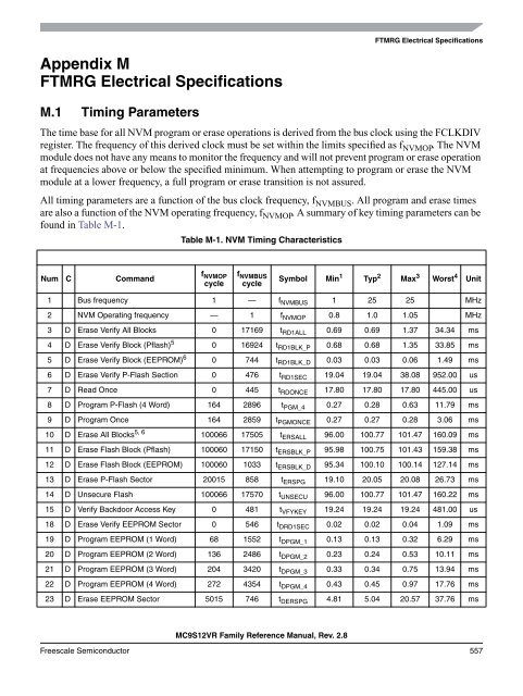
- Page 557 and 558: M.1.1 NVM Reliability Parameters Ta
- Page 559 and 560: Appendix N Package Information MC9S
- Page 561 and 562: MC9S12VR Family Reference Manual, R
- Page 563 and 564: MC9S12VR Family Reference Manual, R
- Page 565 and 566: Appendix O Ordering Information MC9
- Page 567 and 568: Appendix P Detailed Register Addres
- Page 569 and 570: 0x001A-0x001B Part ID Registers MC9
- Page 571 and 572: 0x0034-0x003F Clock Reset and Power
- Page 573 and 574: 0x0070-0x009F Analog to Digital Con
- Page 575 and 576: 0x00A0-0x00C7 Pulse Width Modulator
- Page 577 and 578: MC9S12VR Family Reference Manual, R
- Page 579 and 580: 0x0120 Interrupt Vector Base Regist
- Page 581 and 582: 0x0160-0x0167 LIN Physical Layer (L
- Page 583 and 584: 0x0240 -0x027F Port Integration Mod
- Page 585 and 586: 0x0280-0x02EF Reserved MC9S12VR Fam
- Page 588: How to Reach Us: USA/Europe/Locatio