
You also want an ePaper? Increase the reach of your titles
YUMPU automatically turns print PDFs into web optimized ePapers that Google loves.
locate the memory "cell" that is to be involved in the transfer. In this<br />
case, the cell is an 8-bit word or byte.<br />
The "bar" over part of the signal notation indicates that when the<br />
signal is a logic zero, a write operation is taking place; and when in<br />
the logic one state, a read operation is taking place. Thus, a single<br />
line controls all of the memory functions. In some 6502-based computer<br />
systems and peripherals, you may see the signal "split," tovide<br />
two memory control signals, memory read ( MEMR or MR),<br />
and memory write ( MEMW or MW). This takes some additional<br />
gating, so in most cases, the R/W signal is used by itself. It is available<br />
at pin 34 on the 6502 microprocessor chip.<br />
You may also see the notation RAM used to incorrectly signify<br />
read/write memory. The acronym RAM stands for random-access<br />
memory. In fact, all of the modern, easy-to-use memory devices are<br />
random access, since one may address one location and then any<br />
other, without having to sequence through all of the locations between<br />
the two addresses.<br />
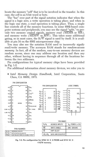
Pin configurations for typical memory chips have been provided<br />
in Fig. 1-2.<br />
For additional information about memory devices, we refer you to<br />
• Intel Memory Design Handbook, Intel Corporation, Santa<br />
Clara, CA 95051, 1975.<br />
PIN CONFIGURATION<br />
24<br />
Vee<br />
PIN CONFIGURATION<br />
LOGIC SYMBOL<br />
M2708<br />
As<br />
Ag Ill<br />
Vee<br />
CS/WE<br />
\\Jo<br />
PROGRAM<br />
Os<br />
A s<br />
A5<br />
A4<br />
A3<br />
A o<br />
A1<br />
A 1<br />
cs<br />
GND<br />
A<br />
1 18 Vee<br />
o<br />
A1<br />
2 17 A i 1101<br />
A<br />
3 16 z<br />
A s<br />
A3<br />
4 2114 15 Ag<br />
A4<br />
1102<br />
5 14 1101<br />
6 13 1102<br />
A 1/03<br />
7 12 1/03<br />
s<br />
A<br />
8 11 1/04<br />
i<br />
A<br />
1/04<br />
9 10 WE<br />
s<br />
cs<br />
A5<br />
A 9 WE<br />
05<br />
04<br />
03<br />
A o -A 9<br />
PIN NAMES<br />
ADDRESS INPUTS<br />
Vee POWER (+5V)<br />
PIN NAMES<br />
Ao·A9 ADDRESS INPUTS<br />
01-0e DATA OUTPUTS/INPUTS<br />
CS/WE CHIP SELECT/WRITE ENABLE INPUT<br />
WE WRITE ENABLE GND GROUND<br />
cs CHIP SELECT<br />
1101-1/04 DATA INPUT/OUTPUT<br />
Fig. 1·2. Pin configuration for 2708 lK X 8 PROM and 2114 lK X<br />
4 R/W memory.<br />
13