
Create successful ePaper yourself
Turn your PDF publications into a flip-book with our unique Google optimized e-Paper software.
power buses, and that the proper connections are made to th<br />
SN7400 chip.<br />
The SN7 400 chip is used to gate the read/ write ( R/ W) signal wi<br />
the main clock signal of the 6502 processor, Q°)l. This gating generat<br />
the memory read signal, RD, and the memory write signal, WR. I<br />
this gating is not done, the computer peripherals on the interface<br />
breadboard will not work properly. In some computers, there<br />
separate read and write signals. If you wish to use separate read<br />
write signals for memory control in the Apple and other ""''"1-'''-'L'o•.<br />
systems that are based on the 6502 microprocessor chip, you<br />
generate them through the proper gating.<br />
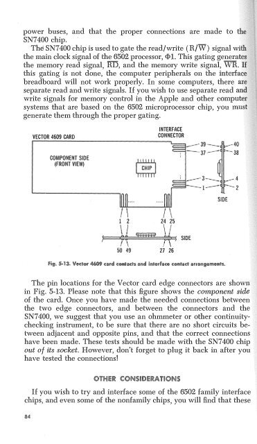
VECTOR 4609 CARD<br />
INTERFACE<br />
CONNECTOR<br />
COMPONENT SIDE<br />
(FRONT VIEW)<br />
I \<br />
24 25<br />
\ I<br />
::· )<br />
!\<br />
27 26<br />
SIDE<br />
The pin locations for the Vector card edge connectors are shown<br />
in Fig. 5-13. Please note that this :Hgure shows the component side<br />
of the card. Once you have made the needed connections between<br />
the two edge connectors, and between the connectors and the<br />
SN7 400, we suggest that you use an ohmmeter or other continuitychecking<br />
instrument, to be sure that there are no short circuits between<br />
adjacent and opposite pins, and that the correct connections<br />
have been made. These tests should be made with the SN7 400 chip<br />
out of its socket. However, don't forget to plug it back in after you<br />
have tested the connections!<br />
If you wish to try and interface some of the 6502 family interface<br />
chips, and even some of the nonfamily chips, you will :find that these