
Create successful ePaper yourself
Turn your PDF publications into a flip-book with our unique Google optimized e-Paper software.
will now explore the actions that each of these software commands<br />
causes to take place.<br />
The PEEK and POKE instructions operate in a very similar manner.<br />
In each, an address is specified, requiring 16 bits of information.<br />
During the execution of either instruction, the address information<br />
contained within the command is transferred to external devices<br />
on the address-bus lines, Al5-AO. In this way, the 1/0 device address<br />
is available to all of the devices and circuits that are connected to<br />
these address lines, both memory and I/ 0 devices.<br />
When a POKE instruction is used in a program, the data value is<br />
also output by the 6502 chip, but on the data-bus lines, D7-DO. Once<br />
the data bits and the address bits are "stable" or present on their respective<br />
buses in useable form, the 6502 asserts the READ/WRITE<br />
signal on the control bus. This synchronizes the acquisition of the<br />
data by the I/0 device that was addressed. Of course, external circuitry<br />
is required to "capture" the data, as well as to identify the selected<br />
I/ 0 device and synchronize it with the 6502-based system. A<br />
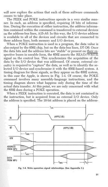
timing diagram for these signals, as they appear on the 6502 system,<br />
in this case the Apple, is shown in Fig. 1-4. Of course, the POKE<br />
command involves many assembly-language instructions, and the<br />
timing diagram shows what happens only during the time of the<br />
actual data transfer. At this point, we are only concerned with what<br />
the 6502 does during a POKE operation.<br />
When a PEEK instruction is executed, the data is not contained in<br />
the instruction, but is acquired from an external I/0 device. Only<br />
the address is specified. The 16-bit address is placed on the address-<br />
i---Tcvc ----i<br />
01<br />
(APPLE 01)<br />
02<br />
(APPLE 00)<br />
DATA<br />
FROM MPU<br />
Fig. 1-4. Write operation signal relationships. (See Appendix C.)<br />
21