

Complete Report - University of New South Wales
Complete Report - University of New South Wales
Complete Report - University of New South Wales
- No tags were found...

Create successful ePaper yourself
Turn your PDF publications into a flip-book with our unique Google optimized e-Paper software.
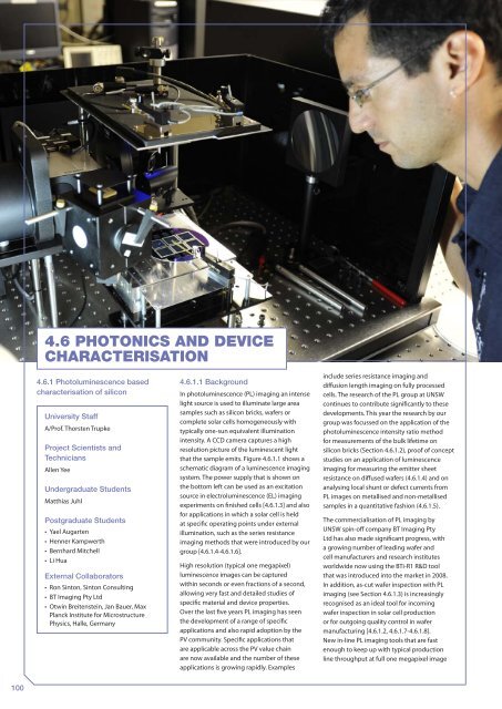
ARCPHOTOVOLTAICSCENTRE OFEXCELLENCE2010/11ANNUAL REPORT4.6 Photonics and deviceCHARACTERISATION4.6.1 Photoluminescence basedcharacterisation <strong>of</strong> silicon<strong>University</strong> StaffA/Pr<strong>of</strong>. Thorsten TrupkeProject Scientists andTechniciansAllen YeeUndergraduate StudentsMatthias JuhlPostgraduate Students• Yael Augarten• Henner Kampwerth• Bernhard Mitchell• Li HuaExternal Collaborators• Ron Sinton, Sinton Consulting• BT Imaging Pty Ltd• Otwin Breitenstein, Jan Bauer, MaxPlanck Institute for MicrostructurePhysics, Halle, Germany4.6.1.1 BackgroundIn photoluminescence (PL) imaging an intenselight source is used to illuminate large areasamples such as silicon bricks, wafers orcomplete solar cells homogeneously withtypically one-sun equivalent illuminationintensity. A CCD camera captures a highresolution picture <strong>of</strong> the luminescent lightthat the sample emits. Figure 4.6.1.1 shows aschematic diagram <strong>of</strong> a luminescence imagingsystem. The power supply that is shown onthe bottom left can be used as an excitationsource in electroluminescence (EL) imagingexperiments on finished cells [4.6.1.3] and als<strong>of</strong>or applications in which a solar cell is heldat specific operating points under externalillumination, such as the series resistanceimaging methods that were introduced by ourgroup [4.6.1.4-4.6.1.6].High resolution (typical one megapixel)luminescence images can be capturedwithin seconds or even fractions <strong>of</strong> a second,allowing very fast and detailed studies <strong>of</strong>specific material and device properties.Over the last five years PL imaging has seenthe development <strong>of</strong> a range <strong>of</strong> specificapplications and also rapid adoption by thePV community. Specific applications thatare applicable across the PV value chainare now available and the number <strong>of</strong> theseapplications is growing rapidly. Examplesinclude series resistance imaging anddiffusion length imaging on fully processedcells. The research <strong>of</strong> the PL group at UNSWcontinues to contribute significantly to thesedevelopments. This year the research by ourgroup was focussed on the application <strong>of</strong> thephotoluminescence intensity ratio methodfor measurements <strong>of</strong> the bulk lifetime onsilicon bricks (Section 4.6.1.2), pro<strong>of</strong> <strong>of</strong> conceptstudies on an application <strong>of</strong> luminescenceimaging for measuring the emitter sheetresistance on diffused wafers (4.6.1.4) and onanalysing local shunt or defect currents fromPL images on metallised and non-metallisedsamples in a quantitative fashion (4.6.1.5).The commercialisation <strong>of</strong> PL imaging byUNSW spin-<strong>of</strong>f company BT Imaging PtyLtd has also made significant progress, witha growing number <strong>of</strong> leading wafer andcell manufacturers and research institutesworldwide now using the BTi-R1 R&D toolthat was introduced into the market in 2008.In addition, as-cut wafer inspection with PLimaging (see Section 4.6.1.3) is increasinglyrecognised as an ideal tool for incomingwafer inspection in solar cell productionor for outgoing quality control in wafermanufacturing [4.6.1.2, 4.6.1.7-4.6.1.8].<strong>New</strong> in-line PL imaging tools that are fastenough to keep up with typical productionline throughput at full one megapixel image100


