

Complete Report - University of New South Wales
Complete Report - University of New South Wales
Complete Report - University of New South Wales
- No tags were found...

Create successful ePaper yourself
Turn your PDF publications into a flip-book with our unique Google optimized e-Paper software.
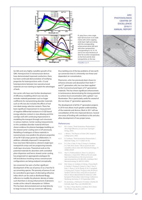
PL enhancementPL Enhancement76no MNP (a) Front10nm Ag14nm Ag18nm Ag522nm Ag43210600 700 800 900 1000Wavelength (nm)20no MNP (b) Rear18Ag reflector10nm Ag1614nmAg18nm Ag1422nm Ag121086420600 700 800 900Wavelength (nm)10001.00.90.80.70.60.50.40.30.20.10.03.22.82.42.01.61.2PL (a.u)PL (a.u)0.80.40.0PL plots from a 4nm singlelayer QD structure in an oxidematrix with a 6nm cappingoxide layer (right axis) alongwith the correspondingenhancement plots (left axis)with silver nanoparticlescorresponding to 10, 14, 18and 22 nm mass thickness <strong>of</strong>silver for (a) silver nanoparticleson the front and (b) silvernanoparticles on the rear.Figure 4.5.71ARCPHOTOVOLTAICSCENTRE OFEXCELLENCE2010/11ANNUAL REPORTGe QDs and very highly crystalline growth <strong>of</strong> GeQWs. Homojunction Si nanostructure deviceshave demonstrated improved conduction, therehas been continued demonstration <strong>of</strong> rectifyingproperties for heterojunctions with c-Si andheterojunctions between two nanostructuredmaterials are now starting to exploit the advantages<strong>of</strong> both.Hot carrier cells have seen further development<strong>of</strong> efficiency modelling which now not onlyincludes material parameters such as Augercoefficients for real promising absorber materialssuch as InN, but also includes the effects <strong>of</strong> realnon-ideal energy selective contacts. There hasbeen significant improvement in measurement<strong>of</strong> negative differential resistance in Si QD basedenergy selective contacts is now allowing and thisoverlaps well with continuing improvement inmodelling the transport through such structuresin various matrices. Carrier cooling measurementson the candidate absorber material InN haveshown evidence for phonon bandgaps building onthe slowed carrier cooling seen in InP previously.Modelling <strong>of</strong> analogues <strong>of</strong> these materials innanostructures now predicts the phonon properties<strong>of</strong> rea lIII-V QD arrays grown by collaborators. Inaddition colloidally dispersed Si nanoparticleshave now been fabricated as coherent single layernanoparticle arrays and are progressing towardsmulti-layer structures. Theoretical work on thepotential materials for absorbers with controlledphon dispersion and hence slowed carrier coolinghas progressed on approapratie analogues forInN and devices involving various nanostructureconfigurations are being analysed conceptually.Up-conversion has seen a further significantdevelopment <strong>of</strong> the use <strong>of</strong> porous-Si as a host for Erup converting species. The porosity <strong>of</strong> porous-Si canbe controlled to give layers <strong>of</strong> alternating refractiveindex which can be used as distributed Braggreflectors to modifiy the photonic density <strong>of</strong> statessuch that there is strong enhancement <strong>of</strong> photonicmodes at the critical Er absorption at 1500nm.This has been demonstrated and can lead directlyto large increase in the up-conversion efficiency,thus tackling one <strong>of</strong> the key problems <strong>of</strong> rare earthup-conversion that it is inherently non-linear anddependent on concentration.Plasmonics, whic has previously been shown toenhance emission and absorption from both 1 stand 2 nd generation cells, has now been appliedto the Si annostructured layers <strong>of</strong> 3 rd generatrionmaterials. This has shown significant enhancementin luminescence demonstrating the strong potentialto achieve local concentration with a global 1 sunillumination. This is particularly useful for several <strong>of</strong>the non-linear 3 rd generation approaches.The development <strong>of</strong> all the 3 rd generation projectsin 2010 now allows much greater understanding<strong>of</strong> the materials and devices. Work in 2011 will seeconsolidation <strong>of</strong> this into improved devices. Severalnew areas <strong>of</strong> funding will contribute to this and alsoallow development <strong>of</strong> new project areas.References:4.5.1 M. A. Green, “Third Generation Photovoltaics:Ultra-High Efficiency at Low Cost” (Springer-Verlag, 2003).4.5.2 J. Nelson, “The Physics <strong>of</strong> Solar Cells”, ImperialCollege press, 2003.4.5.3 G. Conibeer, “Third Generation Photovoltaics”,Materials Today, 10 (11) (2007) 42-50.4.5.4 E-C. Cho, S. Park, X. Hao, D. Song, G. Conibeer,S-C. Park, M.A. Green, “Silicon quantum dot/crystalline silicon solar cells”, Nanotechnology, 19(2008) 2452014.5.5 Hao X J, Podhorodecki A, Shen Y S, Zatryb G,Misiewicz J, Green M A, “Effects <strong>of</strong> Si-rich oxidelayer stoichiometry on the structural andoptical properties <strong>of</strong> Si QDs/SiO 2multilayer film”,Nanotechnology 20, 485703 (2009).4.5.6 M.A. Green, G. Conibeer, D. König, I. Perez-Wurfl,A. Gentle, S. Huang, D. Song, X.J. Hao, F. Gao, S.Park, C. Flynn, Y. So, B. Zhang, D. Di, P. Campbell,Y. Huang and T. Puzzer, “Progress with All-SiliconTandem Cells On Glass Using Silicon QuantumDots in Silicon-Based Dielectric Matrices”, 24thEuropean Photovoltaic Solar Energy Conference,Hamburg, Germany, 21-25 September 2009.4.5.7 M. Zacharias, J. Heitmann, R. Scholz, U. Kahler, M.Schmidt, Appl. Phys. Lett. 80(2002) 661.4.5.8 X.J. Hao, I. Perez-Wurfl, G. Conibeer, M.A. Green,19th PVSEC, Korea, Nov 2009.97


