

Complete Report - University of New South Wales
Complete Report - University of New South Wales
Complete Report - University of New South Wales
- No tags were found...

Create successful ePaper yourself
Turn your PDF publications into a flip-book with our unique Google optimized e-Paper software.
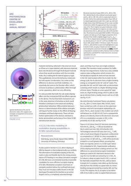
ARCPHOTOVOLTAICSCENTRE OFEXCELLENCE2010/11ANNUAL REPORTElectronic density <strong>of</strong> states (DOS) <strong>of</strong> Si 10QD in 2 MLSiO 2(dotted black), fully oxidised nanocrystal (grey)and Si 10QD in 2 ML SiO 2with Sc replacing Si atom inthe SiO 2shell at the outermost position (top). DOS <strong>of</strong>Sc-doped approximants split into α (spin up, red) andβ (spin down, blue) DOS because <strong>of</strong> non-even number<strong>of</strong> electrons within the approximant due to acceptorstate <strong>of</strong> Sc. The b-highest occupied molecular orbital(HOMO) 1193 indicated in magenta can take up 0.07electrons from the Si 10QD over two 2 ML (6 Å) <strong>of</strong> perfectSiO 2. The β-lowest unoccupied MO (LUMO) 1194 shownin green can take up a much bigger proportion <strong>of</strong> anelectron if the Si QD is slightly bigger (e.g. Si 35, d QD=11 Å). The Sc-doped nanocrystals are shown with theiso-density plots <strong>of</strong> 1.35×10 −3 e/Å 3 for β-HOMO 1193(lower left) and β-LUMO 1194 (lower right). The atoms<strong>of</strong> the Si 10QD and the Sc atom are highlighted in cyan.Si atoms in SiO 2are grey, O atoms are red, H-atomsterminating the outermost O-bonds are white. All DFTcomputations carried out with a Hartree-Fock 3-21G(d)optimisation and B3LYP/6-31G(d) electronic structurecalculation [4.5.23].Figure 4.5.42Spatial distribution <strong>of</strong> 4s and 3delectronic states <strong>of</strong> Sc (upper) andenergetic arrangement <strong>of</strong> 4s and 3dstates (lower).Figure 4.5.41material and being collected in the external circuitas if from an n-type material, with electrons injectedback into the device through the B doped materialwhere they would recombine with the immobileholes, thus making the B material appear p-type.This qualitatively mirrors the behaviour observed,but will require corroboration. As it relies on thedifference in electron and hole mobilities, it isessentially the same as the Dember effect, whichis known to produce a photovoltaic effect throughcarrier separation, albeit not very efficiently.It is also possible that both the sub-oxide dopingeffect and the mismatched QD size effects operatein the device. The fact that both mechanisms actin the same direction is fortuitous as both couldtherefore contribute to the observed rectifyingphotovoltaic behaviour. Differentiation betweenthese or a determination <strong>of</strong> the relative strengthswill require further study on the effects <strong>of</strong> doping,interlayers and band alignments. These will als<strong>of</strong>urther optimisation <strong>of</strong> the devices and lead tobetter photovoltaic performance from these Si QDnanostructure devices.4.5.2.5.2 Ab-initio modelling <strong>of</strong>modulation doping possibilities inSi QDs nanostructuresResearchers:Dirk König, James Rudd, Daniel Hiller (IMTEK,<strong>University</strong> <strong>of</strong> Freiburg, Germany)As discussed in Section 4.5.2.5, direct doping <strong>of</strong>QDs by dopants is thermodynamically very unlikely.The alternative <strong>of</strong> modulation doping <strong>of</strong> the SiO 2matrix is also not feasible due to the strong anionicnature <strong>of</strong> O leading to very deep ionisation energies[4.5.48]. We have concentrated recently on possiblecandidates for more efficienct acceptor doping<strong>of</strong> Si QDs. Modulation acceptors must have anenergetic position below the confined hole level,they must not introduce defect levels in the QDband gap if located at the interface as an activedopant and as a completely saturated foreignatom, and they must have one single oxidationnumber. The transition metal scandium (Sc) fulfilsthe last two requirements. It also has a very suitablevalence state configuration which consists <strong>of</strong> afull (doubly occupied) 4s shell and one electronin the 3d 1 state located within the 4s shell. On theenergy scale, the 4s electrons have a higher bindingenergy as compared to the 3d 1 and 3d 2 states. Thisprovides the 3d 1 and 3d 2 states with an electrostaticscreening which results in a higher binding energy<strong>of</strong> these states. Thereby an unoccupied 3d 2 stateexists at a high binding energy which is able to takeup an electron from a nearby source such as a Si QD,see Fig. 4.5.41.Ab-initio Density Functional Theory calculationson a Si 10QD in 2 mono layers (MLs) <strong>of</strong> SiO 2havebeen carried out, with a Si atom at the outermostposition with full O termination replaced by a Scatom. The Si 10atom cluster is the smallest size whichstill behaves as a Si QD [4.5.23]. Such a nanoparticleallows us to directly observe the electronic structure<strong>of</strong> Sc as a modulation acceptor in SiO 2in theproximity <strong>of</strong> a Si QD, see Fig. 4.5.42.Figure 4.5.42 shows that 0.07 electrons stemmingfrom the Si 10QD (d QD= 7.3Å) are localized atthe Sc atom over two 2 ML (6 Å) <strong>of</strong> perfect SiO 2.Technological relevant QD sizes start at d QD≈ 20Å,with a much lesser degree <strong>of</strong> quantum confinementas compared to a 7.3Å QD. It is thus reasonable toassume that a Si QD with d QD≥ 20Å will be positivelyionized to a much greater extent, ensuring thatholes are majority carriers in a Si QD super lattice(SL) embedded in SiO 2. Experimental verification<strong>of</strong> this doping mechanism is being carried out. Thedifference to conventional acceptor modulationdoping as used in III-V electronic devices is theway the Si or Ge QDs are ionised by Sc in SiO 2. AsSc induces a deep acceptor level in SiO 2it cannotbe thermally ionized from the SiO 2valence band.Instead, the Sc acceptor state takes up the electrondirectly from the initially occupied state at a lowerbinding energy presented by a nearby QD, see Fig.4.5.43. This requires the Sc acceptor to be within50Å <strong>of</strong> the Si QD in order to exploit field emission80


