

Complete Report - University of New South Wales
Complete Report - University of New South Wales
Complete Report - University of New South Wales
- No tags were found...

Create successful ePaper yourself
Turn your PDF publications into a flip-book with our unique Google optimized e-Paper software.
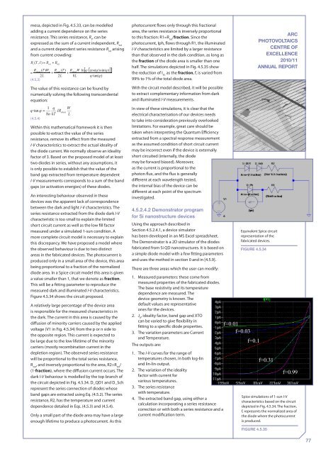
mesa, depicted in Fig. 4.5.33, can be modelledadding a current dependence on the seriesresistance. This series resistance, R S, can beexpressed as the sum <strong>of</strong> a current independent, R extand a current dependent series resistance R intarisingfrom current crowding:(4.5.3)The value <strong>of</strong> this resistance can be found bynumerically solving the following transcendentalequation:(4.5.4)Within this mathematical framework it is thenpossible to extract the value <strong>of</strong> the seriesresistance, remove its effect from the measuredI-V characteristics to extract the actual ideality <strong>of</strong>the diode current. We normally observe an idealityfactor <strong>of</strong> 3. Based on the proposed model <strong>of</strong> at leasttwo diodes in series, without any assumptions, itis only possible to establish that the value <strong>of</strong> theband gap extracted from temperature dependentI-V measurements corresponds to a sum <strong>of</strong> the bandgaps (or activation energies) <strong>of</strong> these diodes.An interesting behaviour observed in thesedevices was the apparent lack <strong>of</strong> correspondencebetween the dark and light I-V characteristics. Theseries resistance extracted from the diode dark I-Vcharacteristic is too small to explain the limitedshort circuit current as well as the low fill factormeasured under a simulated 1-sun condition. Amore complete circuit model is necessary to explainthis discrepancy. We have proposed a model wherethe observed behaviour is due to two distinctareas in the fabricated devices. The photocurrent isproduced only in a small area <strong>of</strong> the device, this areabeing proportional to a fraction <strong>of</strong> the normalizeddiode area. In a Spice circuit model this area is givena value smaller than 1, that we denote as fraction.This will be a fitting parameter to reproduce themeasured dark and illuminated I-V characteristics.Figure 4.5.34 shows the circuit proposed.A relatively large percentage <strong>of</strong> the device areais responsible for the measured characteristics inthe dark. The current in this area is caused by thediffusion <strong>of</strong> minority carriers caused by the appliedvoltage (V1 in Fig. 4.5.34) from the p or n side tothe opposite region. This current is expected tobe large due to the low lifetime <strong>of</strong> the minoritycarriers (mostly recombination current in thedepletion region). The observed series resistancewill be proportional to the total series resistance,R tot, and inversely proportional to the area, R2=R tot/(1-fraction), where the diffusion current occurs. Thedark I-V behaviour is modelled by the top branch <strong>of</strong>the circuit depicted in Fig. 4.5.34. D_QD1 and D_Schrepresent the series connection <strong>of</strong> diodes whoseband gaps are extracted using Eq. (4.5.2). The seriesresistance, R2, has the temperature and currentdependence detailed in Eqs. (4.5.3) and (4.5.4).Only a small part <strong>of</strong> the diode area may have a largeenough lifetime to produce a photocurrent. As thisphotocurrent flows only through this fractionalarea, the series resistance is inversely proportionalto this fraction: R1=R tot/fraction. Since thephotocurrent, Iph, flows through R1, the illuminatedI-V characteristics are limited by a larger resistancethan that observed in the dark condition, as long asthe fraction <strong>of</strong> the diode area is smaller than onehalf. The simulations depicted in Fig. 4.5.35 showthe reduction <strong>of</strong> I SCas the fraction, f, is varied from99% to 1% <strong>of</strong> the total diode area.With the circuit model described, it will be possibleto extract complementary information from darkand illuminated I-V measurements.In view <strong>of</strong> these simulations, it is clear that theelectrical characterisation <strong>of</strong> our devices needsto take into consideration previously overlookedlimitations. For example, great care should betaken when interpreting the Quantum Efficiencyextracted from a spectral response measurementas the assumed condition <strong>of</strong> short circuit currentmay be incorrect even if the device is externallyshort circuited (internally, the diodemay be forward biased). Moreover,as the current is proportional to thephoton flux, and the flux is generallydifferent at each wavelength tested,the internal bias <strong>of</strong> the device can bedifferent at each point <strong>of</strong> the spectruminvestigated.4.5.2.4.2 Demonstrator programfor Si nanostructure devicesUsing the approach described inSection 4.5.2.4.1, a device simulatorhas been developed in an MS Excel spreadsheet.The Demonstrator is a 2D simulator <strong>of</strong> the diodesfabricated from Si QD nanostructures. It is based ona simple diode model with a few fitting parametersand uses the method in section 0 and in [4.5.9].There are three areas which the user can modify:1. Measured parameters: these come frommeasured properties <strong>of</strong> the fabricated diodes.The base resistivity and its temperaturedependence are measured. Thedevice geometry is known. Thedefault values are representativeones for the devices.2. J 0, ideality factor, band gap and XTOcan be varied to give flexibility infitting to a specific diode properties.3. The variation parameters are Currentand Temperature.The outputs are:1. The I-V curves for the range <strong>of</strong>temperatures chosen, in both log-linand lin-lin output.2. The variation <strong>of</strong> the idealityfactor with current forvarious temperatures.3. The series resistancewith temperature.4. The extracted band gap, using either acalculation incorporating a series resistancecorrection or with both a series resistance and acurrent modification term.f=0.01f=0.03ARCPHOTOVOLTAICSCENTRE OFEXCELLENCE2010/11ANNUAL REPORTEquivalent Spice circuitrepresentation <strong>of</strong> thefabricated devices.Figure 4.5.34f=0.1f=0.31f=0.99Spice simulations <strong>of</strong> 1-sun I-Vcharacteristics based on the circuitdepicted in Fig. 4.5.34. The fraction,f, represents the normalized area <strong>of</strong>the diode where the photocurrentis produced.Figure 4.5.3577


