

Complete Report - University of New South Wales
Complete Report - University of New South Wales
Complete Report - University of New South Wales
- No tags were found...

You also want an ePaper? Increase the reach of your titles
YUMPU automatically turns print PDFs into web optimized ePapers that Google loves.
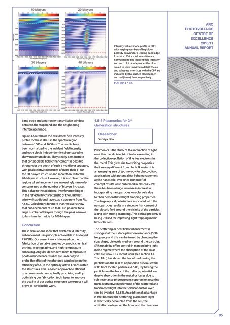
Intensity-valued mode pr<strong>of</strong>ile in DBRswith varying numbers <strong>of</strong> high/lowporositybilayers for a leading band edgefixed at ~1550nm. All intensities arenormalized to the incident field intensityand each plot is independently colorscaledto show maximum detail. The airand substrate interfaces with the DBR areindicated by the dashed black (upper)and red (lower) lines, respectively.ARCPHOTOVOLTAICSCENTRE OFEXCELLENCE2010/11ANNUAL REPORTFigure 4.5.69band edge and a narrower transmission windowbetween the stop band and the neighboringinterference fringe.Figure 4.5.69 shows the calculated field intensitypr<strong>of</strong>ile for these DBRs in the spectral regionbetween 1500 and 1600nm. The results havebeen normalized to the incident field intensityand each plot is independently colour-scaled toshow maximum detail. They clearly demonstratethat considerable field enhancement is possiblethroughout the depth <strong>of</strong> such a multilayer structure,with peak relative intensities <strong>of</strong> more than 11 forthe 30-bilayer structure and more than 18 for the40-bilayer structure. However, it is also clear that theregions <strong>of</strong> enhancement are increasingly narrowlyconcentratedas the number <strong>of</strong> bilayers increases.This is due to the additional interference fringesin the reflectivity characteristic <strong>of</strong> the DBR thatarise with additional layers, as is apparent from Fig.4.5.69. Calculations for more than 40 layers showthat enhancements <strong>of</strong> up to 80 are possible for alarge number <strong>of</strong> bilayers though the peak narrowsto less than 1nm wide for 100 bilayers.ConclusionThese simulations show that drastic field intensityenhancement is in principle achievable in Er-dopedPSi DBRs. Our current work is focused on thefabrication <strong>of</strong> suitable samples by anodic chemicaletching, electroplating, and high-temperatureannealing. Angular-dependent room temperaturephotoluminescence studies are underway toprobe the effect <strong>of</strong> the photonic band edge on theefficiency <strong>of</strong> UC in the optically-active Er ions withinthe structures. This Si-based approach to efficientup-conversion is conceptually promising and byoptimising our fabrication techniques to improvethe quality <strong>of</strong> our optical structures we expect it willprove to be valuable work.4.5.5 Plasmonics for 3 rdGeneration structuresResearcher:Supriya PillaiPlasmonics is the study <strong>of</strong> the interaction <strong>of</strong> lighton a thin metal dielectric interface resulting inthe collective oscillation <strong>of</strong> the free electrons inthe metal. This gives rise to exciting propertiesthat are very different from the bulk metal. It isan emerging area <strong>of</strong> technology for photovoltaicapplications with potential for light managementat the nanoscale. Ever since our pro<strong>of</strong>-<strong>of</strong>concept results were published in 2007 [4.5.79],there has been a huge increase in interest inincorporating nanoparticles on solar cells dueto their demonstrated light trapping properties.The large optical polarisation associated with thenanoparticles results in a strong enhancement <strong>of</strong>the electric field around the vicinity <strong>of</strong> the particlesalong with strong scattering. This optical property isbeing utilised for improving light trapping in thinfilmsolar cells.The scattering or near field enhancement isstrongest at the surface plasmon resonance (SPR)frequency and this can be tuned by changing thesize, shape, dielectric medium around the particles.SPR tunability <strong>of</strong>fers control in manipulating lightin the regime where the absorption <strong>of</strong> the solarcells are weak. Our recent work (see section 4.4Thin Film) has shown the benefits <strong>of</strong> having theparticles on the rear as opposed to previous workwith front located particles [4.5.80]. By having theparticles on the back <strong>of</strong> the cell any potential lossdue to absorption in the metal or losses due tosub-resonance photocurrent suppression resultingfrom destructive interference <strong>of</strong> the scattered andtransmitted light into the semiconductor layercan be avoided [4.5.81]. An additional advantageis that because the scattering plasmonics layeris electrically decoupled from the cell, theantireflection layer on the front and the plasmons95


