

Complete Report - University of New South Wales
Complete Report - University of New South Wales
Complete Report - University of New South Wales
- No tags were found...

Create successful ePaper yourself
Turn your PDF publications into a flip-book with our unique Google optimized e-Paper software.
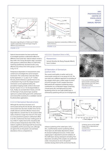
ARCPHOTOVOLTAICSCENTRE OFEXCELLENCE2010/11ANNUAL REPORTAbsorption edge fitting for UT-SiN2.0 and UT-SiN0.2samples respectively, (insert: band gap energy fordifferent Si 3N 4thicknesses).Figure 4.5.19Temperature-depentent conductitity <strong>of</strong> different Si 3N 4barrier thickness.Figure 4.5.20Optical characterization has been performedto investigate quantum confinement effects fordifferent nanocrystal sizes. Optical analysis reveals ablue shift in the strong absorption edge, consistentwith quantum confinement effects in small Si NCsmatching qualitatively calculated results usingeffective mass theory from other groups, as shownin Fig. 4.5.19.Temperature dependent I-V measurements werecarried out to investigate the carrier transportmechanism. The conductivity is best describedby the expression, σ = σ 0exp [-(T 0/T) 1/2 ] whenthe Si 3N 4barrier thickness is greater than 0.5 nm,as illustrated in Fig. 4.5.20. The charge transportmechanism can be explained well by thepercolation-hopping model, similar to the resultfound in Section 4.5.2.3.1 for Sb doped SiQDs inSi 3N 4. Finally, we conclude that in future, a 0.5-0.8nm thick layer <strong>of</strong> Si 3N 4barrier layer would beoptimum to achieve both good Si-NC confinementand minimal film resistivity for a candidate materialfor photovoltaic applications.4.5.2.3.4.1 Quantum Dots in SiO 2Researchers:Santosh Shrestha, Bo Zhang, Pasquale Aliberti,Gavin Conibeer(i) Fabrication <strong>of</strong> Germaniumquantum dotsThe current work builds on earlier work on Genanocrystals carried out in our group [4.5.32]. Thenew work uses a different approach to annealing <strong>of</strong>the samples which gives a wider range <strong>of</strong> control<strong>of</strong> Ge NC formation. Ge NC samples have beenfabricated by RF magnetron sputtering using acombination <strong>of</strong> a combination target comprisinga fused quartz disc and high purity Ge strips.Sputtering <strong>of</strong> the Ge-rich oxide (GeRO) layer isachieved by sputtering with just an Ar background,Cross-section HRTEM image <strong>of</strong> atypical sample containing GeROlayers between GeO 2/SiO 2layersfollowing annealing.Figure 4.5.214.5.2.3.4 Germanium NanostructuresAlthough the main focus has been on Sinanocrystals during the last decade, other group IVnanocrystals have also been studied. Since Ge hassmaller electron and hole effective masses and alarger dielectric constant than Si, the excitonic Bohrradius <strong>of</strong> bulk Ge is larger than that <strong>of</strong> Si. This leadsto a more prominent quantum confinement effectin Ge NCs. Furthermore the lower melting point <strong>of</strong>Ge at 938.3 o C implies that Ge NCs should be ableto form at lower temperatures than Si NCs. This isindeed a significant advantage both for processingcompatibility and for processing costs, althoughset against this are the greater cost and lowerabundance <strong>of</strong> Ge as compared to Si.whereas sputtering <strong>of</strong> the oxide layers, GeO 2/SiO 2, is performed by reactive sputtering with O 2.These layers are alternately deposited to obtainthe desired multilayered structure. A thick oxidecapping layer is deposited to prevent oxidation <strong>of</strong>the GeRO layers during subsequent annealing. Postdeposition annealing <strong>of</strong> the samples was performedunder a low pressure (in-situ in the growthchamber) during which Ge NCs are formed. Results(a) Raman spectra and (b) GIXRDimage <strong>of</strong> the as-deposited andannealed films.Figure 4.5.2271


