

Complete Report - University of New South Wales
Complete Report - University of New South Wales
Complete Report - University of New South Wales
- No tags were found...

You also want an ePaper? Increase the reach of your titles
YUMPU automatically turns print PDFs into web optimized ePapers that Google loves.
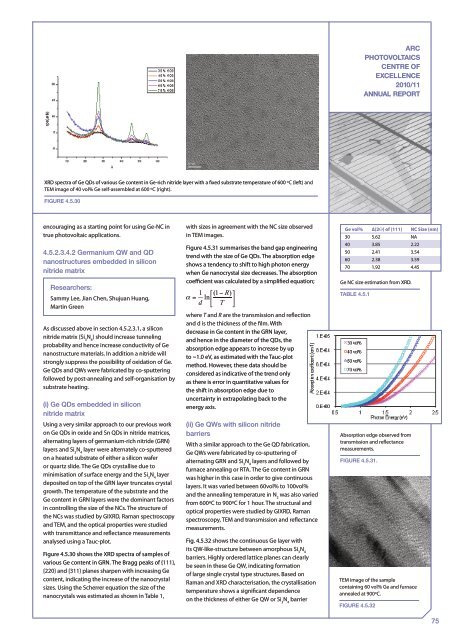
ARCPHOTOVOLTAICSCENTRE OFEXCELLENCE2010/11ANNUAL REPORTXRD spectra <strong>of</strong> Ge QDs <strong>of</strong> various Ge content in Ge-rich nitride layer with a fixed substrate temperature <strong>of</strong> 600 ºC (left) andTEM image <strong>of</strong> 40 vol% Ge self-assembled at 600 ºC (right).Figure 4.5.30encouraging as a starting point for using Ge-NC intrue photovoltaic applications.4.5.2.3.4.2 Germanium QW and QDnanostructures embedded in siliconnitride matrixResearchers:Sammy Lee, Jian Chen, Shujuan Huang,Martin GreenAs discussed above in section 4.5.2.3.1, a siliconnitride matrix (Si 3N 4) should increase tunnelingprobability and hence increase conductivity <strong>of</strong> Genanostructure materials. In addition a nitride willstrongly suppress the possibility <strong>of</strong> oxidation <strong>of</strong> Ge.Ge QDs and QWs were fabricated by co-sputteringfollowed by post-annealing and self-organisation bysubstrate heating.(i) Ge QDs embedded in siliconnitride matrixUsing a very similar approach to our previous workon Ge QDs in oxide and Sn QDs in nitride matrices,alternating layers <strong>of</strong> germanium-rich nitride (GRN)layers and Si 3N 4layer were alternately co-sputteredon a heated substrate <strong>of</strong> either a silicon waferor quartz slide. The Ge QDs crystallise due tominimisation <strong>of</strong> surface energy and the Si 3N 4layerdeposited on top <strong>of</strong> the GRN layer truncates crystalgrowth. The temperature <strong>of</strong> the substrate and theGe content in GRN layers were the dominant factorsin controlling the size <strong>of</strong> the NCs. The structure <strong>of</strong>the NCs was studied by GIXRD, Raman spectroscopyand TEM, and the optical properties were studiedwith transmittance and reflectance measurementsanalysed using a Tauc-plot.Figure 4.5.30 shows the XRD spectra <strong>of</strong> samples <strong>of</strong>various Ge content in GRN. The Bragg peaks <strong>of</strong> {111},{220} and {311} planes sharpen with increasing Gecontent, indicating the increase <strong>of</strong> the nanocrystalsizes. Using the Scherrer equation the size <strong>of</strong> thenanocrystals was estimated as shown in Table 1,with sizes in agreement with the NC size observedin TEM images.Figure 4.5.31 summarises the band gap engineeringtrend with the size <strong>of</strong> Ge QDs. The absorption edgeshows a tendency to shift to high photon energywhen Ge nanocrystal size decreases. The absorptioncoefficient was calculated by a simplified equation;where T and R are the transmission and reflectionand d is the thickness <strong>of</strong> the film. Withdecrease in Ge content in the GRN layer,and hence in the diameter <strong>of</strong> the QDs, theabsorption edge appears to increase by upto ~1.0 eV, as estimated with the Tauc-plotmethod. However, these data should beconsidered as indicative <strong>of</strong> the trend onlyas there is error in quantitative values forthe shift in absorption edge due touncertainty in extrapolating back to theenergy axis.(ii) Ge QWs with silicon nitridebarriersWith a similar approach to the Ge QD fabrication,Ge QWs were fabricated by co-sputtering <strong>of</strong>alternating GRN and Si 3N 4layers and followed byfurnace annealing or RTA. The Ge content in GRNwas higher in this case in order to give continuouslayers. It was varied between 60vol% to 100vol%and the annealing temperature in N 2was also variedfrom 600ºC to 900ºC for 1 hour. The structural andoptical properties were studied by GIXRD, Ramanspectroscopy, TEM and transmission and reflectancemeasurements.Fig. 4.5.32 shows the continuous Ge layer withits QW-like-structure between amorphous Si 3N 4barriers. Highly ordered lattice planes can clearlybe seen in these Ge QW, indicating formation<strong>of</strong> large single crystal type structures. Based onRaman and XRD characterisation, the crystallisationtemperature shows a significant dependenceon the thickness <strong>of</strong> either Ge QW or Si 3N 4barrierGe vol% ∆(2Ө) <strong>of</strong> (111) NC Size (nm)30 5.62 NA40 3.85 2.2250 2.41 3.5460 2.38 3.5970 1.92 4.45Ge NC size estimation from XRD.Table 4.5.1Absorption edge observed fromtransmission and reflectancemeasurements.Figure 4.5.31.TEM image <strong>of</strong> the samplecontaining 60 vol% Ge and furnaceannealed at 900ºC.Figure 4.5.3275


