

Complete Report - University of New South Wales
Complete Report - University of New South Wales
Complete Report - University of New South Wales
- No tags were found...

Create successful ePaper yourself
Turn your PDF publications into a flip-book with our unique Google optimized e-Paper software.
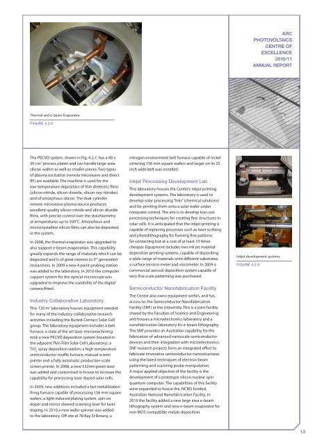
ARCPHOTOVOLTAICSCENTRE OFEXCELLENCE2010/11ANNUAL REPORTThermal and e-beam Evaporator.Figure 4.2.8The PECVD system, shown in Fig. 4.2.7, has a 40 x20 cm 2 process platen and can handle large-areasilicon wafers as well as smaller pieces. Two types<strong>of</strong> plasma excitation (remote microwave and directRF) are available. The machine is used for thelow-temperature deposition <strong>of</strong> thin dielectric films(silicon nitride, silicon dioxide, silicon oxy-nitrides)and <strong>of</strong> amorphous silicon. The dual-cylinder,remote microwave plasma source producesexcellent-quality silicon nitride and silicon dioxidefilms, with precise control over the stoichiometryat temperatures up to 500°C. Amorphous andmicrocrystalline silicon films can also be depositedin the system.In 2008, the thermal evaporator was upgraded toalso support e-beam evaporation. This capabilitygreatly expands the range <strong>of</strong> materials which can bedeposited and is <strong>of</strong> great interest to 3 rd generationresearchers. In 2009 a new 4 point probing stationwas added to the laboratory. In 2010 the computersupport system for the optical microscope wasupgraded to improve the useability <strong>of</strong> the digitalcamera fitted.Industry Collaborative LaboratoryThis 120 m 2 laboratory houses equipment neededfor many <strong>of</strong> the industry-collaborative researchactivities including the Buried-Contact Solar Cellgroup. The laboratory equipment includes a beltfurnace; a state <strong>of</strong> the art laser micromachiningtool; a new PECVD deposition system (located inthe adjacent Thin Film Solar Cell Laboratory); aTiO 2spray deposition station; a high temperaturesemiconductor muffle furnace, manual screenprinter and a fully automatic production scalescreen printer. In 2008, a new 532nm green laserwas added and customised in-house to increase thecapability for processing laser doped solar cells.In 2009, new additions included a fast metallizationfiring furnace capable <strong>of</strong> processing 156 mm squarewafers, a light induced plating system, spin ondoper and mirror steered scanning laser for laserdoping. In 2010 a new wafer spinner was addedto the laboratory. Off site at 78 Bay St Botany, anitrogen environment belt furnace capable <strong>of</strong> nickelsintering 156 mm square wafers and larger on its 25inch wide belt was installed.Inkjet Processing Development LabThis laboratory houses the Centre’s inkjet printingdevelopment systems. The laboratory is used todevelop solar processing “inks” (chemical solutions)and for printing them onto a solar wafer undercomputer control. The aim is to develop low costprocessing techniques for creating fine structures insolar cells. It is anticipated that the inkjet printing iscapable <strong>of</strong> replacing processes such as laser scribingand photolithography for forming fine patternsfor contacting but at a cost <strong>of</strong> at least 10 timescheaper. Equipment includes two ink jet materialdeposition printing systems, capable <strong>of</strong> depositinga wide range <strong>of</strong> materials onto different substrates,a surface tension meter and viscometer. In 2009 acommercial aerosol deposition system capable <strong>of</strong>very fine scale patterning was purchased.Semiconductor Nan<strong>of</strong>abrication FacilityThe Centre also owns equipment within, and hasaccess to, the Semiconductor Nan<strong>of</strong>abricationFacility (SNF) at the <strong>University</strong>. This is a joint facilityshared by the Faculties <strong>of</strong> Science and Engineeringand houses a microelectronics laboratory and anan<strong>of</strong>abrication laboratory for e-beam lithography.The SNF provides an Australian capability for thefabrication <strong>of</strong> advanced nanoscale semiconductordevices and their integration with microelectronics.SNF research projects form an integrated effort t<strong>of</strong>abricate innovative semiconductor nanostructuresusing the latest techniques <strong>of</strong> electron beampatterning and scanning probe manipulation.A major applied objective <strong>of</strong> the facility is thedevelopment <strong>of</strong> a prototype silicon nuclear spinquantum computer. The capabilities <strong>of</strong> this facilitywere expanded to house the, NCRIS funded,Australian National Nan<strong>of</strong>abrication Facility. In2010 the facility added a new large area e-beamlithography system and new e-beam evaporator fornon MOS-compatible metals deposition.Inkjet development systems.Figure 4.2.919


