

Complete Report - University of New South Wales
Complete Report - University of New South Wales
Complete Report - University of New South Wales
- No tags were found...

You also want an ePaper? Increase the reach of your titles
YUMPU automatically turns print PDFs into web optimized ePapers that Google loves.
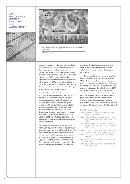
ARCPHOTOVOLTAICSCENTRE OFEXCELLENCE2010/11ANNUAL REPORTSEM cross-section <strong>of</strong> CZTS-type cells (Todorov et al., Adv. Mater. 22,E156, 2010).Figure 4.4.3.2a more attractive process because large area/highrate sputtering is a better developed techniquethan evaporation. In addition, sputtering hascommercially available equipment that gives gooduniformity over large areas. UNSW has considerableexperience in PVD techniques, such as theachievement <strong>of</strong> the first silicon quantum dot solarcell on quartz [4.4.3.3], a recent patent relating tocrystal Ge on Si wafer by a sputtering technique andthe polycrystalline silicon thin film solar cell on glassby an evaporation technique [4.4.3.4].Almost all <strong>of</strong> the methods that have beenattempted for CZTS fabrication involve two steps;deposition <strong>of</strong> a metal/metal-sulfide precursorand a subsequent anneal at high temperaturein a hydrogen sulphide or elemental sulphurenvironment to incorporate more sulfur into thefilm and evolve the correct phase [4.4.3.5-4.4.3.7].It is reported that the H 2S/sulphur anneal is adestructive process that can potentially introducedefects into the film due to the out-diffusion <strong>of</strong>metals. In addition, for large scale production <strong>of</strong>solar cells, a direct one-step, large area depositionprocess is preferred.Fortunately, reactive sputtering is a well suitedtechnique because <strong>of</strong> the above-addressed feature<strong>of</strong> precise control on the stoichiometry <strong>of</strong> depositedfilms over a large area with high uniformity at arelatively low cost. The experience documented inour patent <strong>of</strong> “A Method <strong>of</strong> Forming A GermaniumLayer On A Silicon Substrate And A PhotovoltaicDevice Including A Germanium Layer”, where theintroduction <strong>of</strong> H 2gas into the in-situ depositedgermanium thin film by magnetron sputteringresults in the significant improvement <strong>of</strong> theperformance <strong>of</strong> germanium thin film, appearshighly relevant.As such, the idea <strong>of</strong> one-step reactive sputteringby in-situ introducing H 2S gas into the depositedCZT (Cu 2ZnSn) film is a logical step to attempt abetter CZTS film quality. However, there have beenfew attempts to date at such a simplified one-stepprocess by introducing the sulphide into the CZTSfilm during in-situ deposition. In addition, thisprocess is not well understood and significantlymore effort is required in order to understandgrowth mechanisms involved in the reactivesputtering process. Comparison <strong>of</strong> reactivelysputtered films with 2-step sulphidisation processeswill provide the early emphasis <strong>of</strong> the Centre’s work.4.4.3.3 References4.4.3.1 T.K. Todorov, K.B. Reuter, D.B. Mitzi, AdvancedMaterials 2010, 22, E156.4.4.3.2 W. Liu, D.B. Mitzi, M. Yuan, A.J. Kellock, S.J. Chey,and O. Gunawan, Chem.Mater., 2010, 22(3), 1010-1014.4.4.3.3 I. Perez-Wurfl, X.J. Hao, A .Gentle, D-H. Kim, G.Conibeer, M.A. Green, Applied Physics Letters 95(2009), 153506.4.4.3.4 Z. Ouyang, S. Pillai, F. Beck, O. Kunz, S. Varlamov, etal., Applied Physics Letters, 2010, 96 (26), 261109.4.4.3.5 J.J. Scragg et al., Thin Solid Films, 517 (2009), pp.2481-2484.4.3.3.6 R. Schuee et al., Thin Solid Films, 517 (2009) pp.2465-2468.4.4.3.7 Hironori Katagiri et al., Thin Solid Films, 480-481(2005), pp. 426-432.60


