

Complete Report - University of New South Wales
Complete Report - University of New South Wales
Complete Report - University of New South Wales
- No tags were found...

You also want an ePaper? Increase the reach of your titles
YUMPU automatically turns print PDFs into web optimized ePapers that Google loves.
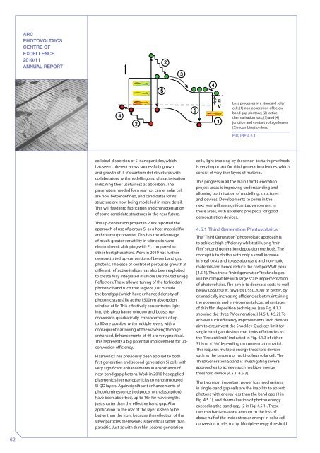
ARCPHOTOVOLTAICSCENTRE OFEXCELLENCE2010/11ANNUAL REPORTLoss processes in a standard solarcell: (1) non-absorption <strong>of</strong> belowband gap photons; (2) latticethermalisation loss; (3) and (4)junction and contact voltage losses;(5) recombination loss.Figure 4.5.1colloidal dispersion <strong>of</strong> Si nanoparticles, whichhas seen coherent arrays successfully grown,and growth <strong>of</strong> III-V quantum dot structures withcollaborators, with modelling and characterisationindicating their usefulness as absorbers. Theparameters needed for a real hot carrier solar cellare now better defined, and candidates for itsstructure are now being modelled in more detail.This will feed into fabrication and characterisation<strong>of</strong> some candidate structures in the near future.The up-conversion project in 2009 reported theapproach <strong>of</strong> use <strong>of</strong> porous-Si as a host material foran Erbium upconverter. This has the advantage<strong>of</strong> much greater versatility in fabrication andelectrochemical doping with Er, compared toother host phosphors. Work in 2010 has furtherdemonstrated up-conversion <strong>of</strong> below band gapphotons. The ease <strong>of</strong> control <strong>of</strong> porous-Si growth atdifferent refractive indices has also been exploitedto create fully integrated multiple Distributed BraggReflectors. These allow a tuning <strong>of</strong> the forbiddenphotonic band such that regions just outsidethe bandgap (which have enhanced density <strong>of</strong>photonic states) lie at the 1500nm absorptionwindow <strong>of</strong> Er. This effectively concentrates lightinto this absorbance window and boosts upconversionquadratically. Enhancements <strong>of</strong> upto 80 are possible with multiple levels, with aconsequent narrowing <strong>of</strong> the wavelength rangeenhanced. Enhancements <strong>of</strong> 40 are very practical.This represents a big potential improvement for upconversionefficiency.Plasmonics has previously been applied to bothfirst generation and second generation Si cells withvery significant enhancements in absorbance <strong>of</strong>near band gap photons. Work in 2010 has appliedplasmonic silver nanoparticles to nanostructuredSi QD layers. Again significant enhancements <strong>of</strong>photoluminescence (reciprocal with absorption)have been absorbed, up to 16x for wavelengthsjust shorter than the effective band gap. Alsoapplication to the rear <strong>of</strong> the layer is seen to bebetter than the front because the reflection <strong>of</strong> thesilver particles themselves is beneficial rather thanparasitic. Just as with thin film second generationcells, light trapping by these non-texturing methodsis very important for third generation devices, whichconsist <strong>of</strong> very thin layers <strong>of</strong> material.This progress in all the main Third Generationproject areas is improving understanding andallowing optimisation <strong>of</strong> modelling, structuresand devices. Developments to come in thenext year will see significant advancement inthese areas, with excellent prospects for gooddemonstration devices.4.5.1 Third Generation PhotovoltaicsThe “Third Generation” photovoltaic approach isto achieve high efficiency whilst still using “thinfilm” second generation deposition methods. Theconcept is to do this with only a small increasein areal costs and to use abundant and non-toxicmaterials and hence reduce the cost per Watt peak[4.5.1]. Thus these “third generation” technologieswill be compatible with large scale implementation<strong>of</strong> photovoltaics. The aim is to decrease costs to wellbelow US$0.50/W, towards US$0.20/W or better, bydramatically increasing efficiencies but maintainingthe economic and environmental cost advantages<strong>of</strong> thin film deposition techniques (see Fig. 4.1.3showing the three PV generations) [4.5.1, 4.5.2]. Toachieve such efficiency improvements such devicesaim to circumvent the Shockley-Queisser limit forsingle band gap devices that limits efficiencies tothe “Present limit” indicated in Fig. 4.1.3 <strong>of</strong> either31% or 41% (depending on concentration ratio).This requires multiple energy threshold devicessuch as the tandem or multi-colour solar cell. TheThird Generation Strand is investigating severalapproaches to achieve such multiple energythreshold device [4.5.1, 4.5.3].The two most important power loss mechanismsin single-band gap cells are the inability to absorbphotons with energy less than the band gap (1 inFig. 4.5.1), and thermalisation <strong>of</strong> photon energyexceeding the band gap, (2 in Fig. 4.5.1). Thesetwo mechanisms alone amount to the loss <strong>of</strong>about half <strong>of</strong> the incident solar energy in solar cellconversion to electricity. Multiple energy threshold62


