

Complete Report - University of New South Wales
Complete Report - University of New South Wales
Complete Report - University of New South Wales
- No tags were found...

Create successful ePaper yourself
Turn your PDF publications into a flip-book with our unique Google optimized e-Paper software.
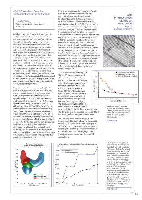
4.5.2.2.2 Modelling <strong>of</strong> quantumconfinement and tunnelling transportResearchers:Binesh Puthen-Veettil, Robert Patterson,Dirk KönigBand gap engineering for these Si nanostructurematerials requires a large number <strong>of</strong> almostidentical quantum dots (QDs), evenly distributedin a dielectric layer. As the proximity <strong>of</strong> dotsincreases, confined wavefunctions in the QDsinteract with one another to form mini-bands. Itis also seen that higher Si content in the Si richlayer gives rise to bigger QDs, due to the tendency<strong>of</strong> QDs to merge together and form bigger dotsduring annealing [4.5.12, 4.5.20]. If the dielectriclayer is a good diffusion barrier for Si (such as thenitride layer in Si/Si 3N 4or Si 3N 4interlayer samples,see sections 4.5.2.3.1 and 4.5.2.3.2), this effect isstrongly reduced. For relatively thick layers in whichdiffusion is not constrained, the shapes <strong>of</strong> theseQDs can differ greatly from an ideal spherical shape.Calculation <strong>of</strong> confined energy in QD structures is <strong>of</strong>interest since their electronic and optical propertiescan be determined by determining the confinedenergy levels in the structure.Since these calculations are extremely difficult toperform using ab-initio methods due to the largememory and computation time requirements,we have developed a model to quantitativelyanalyse electronic states and their interactions ina QD array, in the framework <strong>of</strong> the effective massapproximation (EMA) calibrated by ab-initio DFTcalculations. This model is realized by solving thethree dimensional time independent discretizedSchrödinger’s equation in the EMA, employing amodified Full Multi Grid method (FMG) [4.5.21] toovercome the difficulty <strong>of</strong> computational intensity.By using exact solution methods to solve the Eigenequation for the coarsest grid, the non convergenceproblems [4.5.22] arising from oscillatoryeigenvalues are eliminated. Since initial guesses<strong>of</strong> the solution are very close to the approximatesolution, this method proves to be much faster thanother iterative methods. The flow diagram for thisprocess is shown in Fig. 4.5.5.In order to demonstrate the conformity <strong>of</strong> resultsfrom this model with experimental results,we compared it with experimental resultsfor Silicon QDs in SiO 2dielectric grown usingsputtering methods and characterized usingphotoluminescence (PL) [4.5.20]. Figure 4.5.6 showsthe dependency <strong>of</strong> confined energy on the size<strong>of</strong> QDs for Si/SiO 2QD structures. Confined energyincreases exponentially as QD size decreases.Comparison shows that for larger QDs experimentaland theoretical values are similar, but for smallerdots the experimental results for the confinedenergy shows a lower degree <strong>of</strong> confinementthan the theoretical result. This difference can beattributed to interface defects between Si and SiO 2and to defects within the SiO 2matrix but near theinterface. For QDs below a diameter <strong>of</strong> about 4 nmthese interface effects have a larger influence on theconfined energy level. This is because the groundstate electron density, which is concentrated atthe centre <strong>of</strong> the QD, is closer to these interfacedefects for the smaller QDs and hence morestrongly influenced.As an extreme example <strong>of</strong> irregularlyshaped QD, we have investigatedelectronic states in aribitrarilyshaped QDs. Here we have used the“horseshoe” morphology [4.5.24],formed by lateral growth <strong>of</strong> Si QDinside SiO 2dielectric shown inFigure 4.5.7 (left). These states arefound to be very different from theexpected electronic energy levelsthat are associated with sphericalQDs as shown in Fig. 4.5.7 (right).The degeneracy in spherical QDs (3in first excited level and 5 in secondexcited level) is lost due to the asymmetric shape.The deviation from the expected confinement levelbecomes significant at higher confined levels.This thus indicates the importance <strong>of</strong> knowingthe regime <strong>of</strong> QD growth relevant for the materialconditions. As shown in the TEM tomography <strong>of</strong>Section 4.5.2.2.3, under appropriate conditions <strong>of</strong>Si density and annealing, a spherical morphologycan be maintained and QD merging avoided,thus giving greater control over the confinedenergy levels.ARCPHOTOVOLTAICSCENTRE OFEXCELLENCE2010/11ANNUAL REPORTSimulation results – multigridmethod and Density FunctionalTheory (DFT) calculations [4.5.23]compared with the experimentalresults for Silicon QDs inSiO 2dielectric.Figure 4.5.6First three modes <strong>of</strong> electronicwave-functions in a “horseshoe”shaped QD with high surface tovolume ratio (far left). The groundstate is located near the centre <strong>of</strong>the dot and is approximately in aspherical shape with zero nodes.The number <strong>of</strong> nodes increaseswith the increase in the energylevel. Energy levels associated witha horseshoe shaped QD comparedwith that <strong>of</strong> a 6nm diameterspherical QD (left). The twomorphologies give energies whichare most similar for their groundstates, with the horseshoe shapegiving significantly lower energiesthan spherical for higher confinedlevels. The degeneracy in energylevels is lost in the horseshoeshaped dot.FigurE 4.5.765


