

Complete Report - University of New South Wales
Complete Report - University of New South Wales
Complete Report - University of New South Wales
- No tags were found...

Create successful ePaper yourself
Turn your PDF publications into a flip-book with our unique Google optimized e-Paper software.
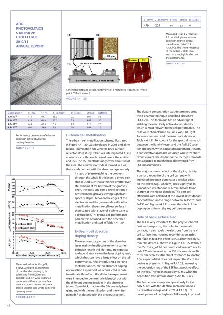
ARCPHOTOVOLTAICSCENTRE OFEXCELLENCE2010/11ANNUAL REPORTV oc(mV) J sc(mA/cm 2 ) FF (%) Eff (%) Rs (Ωcm 2 )479 20.1 66 6.3 4Measured 1 sun J-V results <strong>of</strong>1.8 µm thick planar e-beamcells with aligned bifacialmetallisation ([4.4.1.13,4.4.1.14]). The shunt resistance<strong>of</strong> the cells is > 2000 Ωcm 2and has a negligible effect onthe performance.Table 4.4.1.10Schematic (left) and actual (right) views <strong>of</strong> a metallised e-beam cell (whitepaint BSR not shown).Figure 4.4.1.20Doping (cm -3 ) V oc(mV) FF (%) J sc(mA/cm 2 ) R s(Ωcm 2 ) Eff (%) pEff (%)1.7×10 15 413 64.1 19.2 2.0 5.09 5.55.7×10 15 418 61.9 17.6 3.4 4.67 5.31.0×10 17 449 62.5 6.5 7.9 2.16 2.58.3×10 17 403 54.4 4.0 19 1.04 1.3Performance parameters <strong>of</strong> e-beamcells with different absorberdoping densities.Table 4.4.1.11Measured values for Voc, pFF,J sc(EQE), and pEff as a function<strong>of</strong> the absorber doping. J sciscalculated from EQE results.Jsc(EQE) and pEff were obtainedunder two different back surfacereflector (BSR) schemes: air (blackclosed squares) and white paint (redopen squares).Figure 4.4.1.21E-Beam cell metallisationThe e-beam cell metallisation scheme, illustratedin Figure 4.4.1.20, was developed in 2008 and allowbifacial illumination and versatile back surfacereflector (BSR) study. It features interdigitated Al linecontacts for both heavily doped layers, the emitterand BSF. The BSF electrodes only cover about 4% <strong>of</strong>the area. The emitter electrode is formed in a waythat avoids contact with the absorber layer entirely.Instead <strong>of</strong> plasma etching the groovesthrough the whole Si thickness, a timed etchstop is used such that a thinned emitter layerstill remains at the bottom <strong>of</strong> the grooves.Then, the glass-side comb-like electrode iscentred in the grooves leaving significantspace (>10 μm) between the edges <strong>of</strong> theelectrodes and the groove sidewalls. Aftermetallisation the entire cell rear surface isthen coated with a layer <strong>of</strong> a white paint asa diffuse BSR. The typical cell performanceparameters obtained with the describedmetallisation are listed in Table 4.4.1.10.E-Beam cell absorberdoping densityThe electronic properties <strong>of</strong> the absorberlayer, mainly the effective minority carrierdiffusion length and life-time, are expectedto depend strongly on the layer doping level,which thus can have a large effect on the cellperformance. After introducing a workingmetalisation scheme, an absorber dopingoptimisation experiment was conducted in orderto estimate this effect. All cells in the experimentwere intended to be nominally identical but withthe different doping densities in the absorber(about 2 μm thick, made on the SiN coated planarglass, and with the metallisation and the whitepaintBSR as described in the previous section).The dopant concentration was determined usingthe Z-analysis technique described elsewhere[4.4.1.27]. This technique has an advantage <strong>of</strong>yielding the electrically active dopant density,which is most relevant to the cell performance. Thecells were characterised by Suns-Voc, EQE, lightJ-V measurements and the results are shown inTable 4.4.1.11. To account for the spectral mismatchbetween the light I-V tester and the AM1.5G solartest spectrum, which causes measurement artifacts,a conservative approach was used where the shortcircuitcurrent density during the J-V measurementswas adjusted to match those determined fromEQE measurements.The major observed effect <strong>of</strong> the doping densityis a sharp reduction <strong>of</strong> the cell current withincreased doping. It dominates a weaker effecton the cell voltage, where V ocrises slightly up todopant density <strong>of</strong> about 1e17/cm 3 before fallingsharply at the higher densities. The best cellefficiencies are obtained at the lowest active dopantconcentrations in the range between 1e15/cm 3 and5e15/cm 3 . Figure 4.4.1.21 shows the effect <strong>of</strong> thedoping densities on the key cell parameters.Role <strong>of</strong> back surface filedThe BSF is very important for the poly-Si solar cell.Besides transporting the holes to the metalliccontacts, it also repels the electrons from the rearcell surface thus reducing recombination at thisinterface. In fact, this effect is crucial for the poly-Sithin-film device as shown in Figure 4.4.1.22. Withoutthe BSF the V oc<strong>of</strong> the cell is reduced from 435 mV toonly 270 mV. Increasing the BSF thickness from 30to 90 nm decreases the sheet resistance by a factor3 (as expected) but does not impact the Voc <strong>of</strong> thedevice as presented in Figure 4.4.1.22. Increasingthe deposition rate <strong>of</strong> the BSF has a positive effecton the Voc. The Voc increases by 40 mV when thedeposition rate increases from 5 A/s to 10 A/s.The best efficiency reported previously for thepoly-Si cell with the identical metallization was5.2 % with a voltage <strong>of</strong> 435 mV [4.4.1.13]. Thedevelopment <strong>of</strong> the high rate BSF clearly improved46


