

Complete Report - University of New South Wales
Complete Report - University of New South Wales
Complete Report - University of New South Wales
- No tags were found...

Create successful ePaper yourself
Turn your PDF publications into a flip-book with our unique Google optimized e-Paper software.
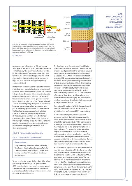
ARCPHOTOVOLTAICSCENTRE OFEXCELLENCE2010/11ANNUAL REPORTA tandem photovoltaic cell using quantum confined QDs or QWsto engineer the band gap <strong>of</strong> the top cell and potentially also thelower cells. Short wavelength light is absorbed in the top cell andlonger wavelengths in lower cells, thus boosting the overall voltagegenerated and hence efficiency.Figure 4.5.2approaches can utilise some <strong>of</strong> this lost energy.Such approaches do not in fact disprove the validity<strong>of</strong> the Shockley-Queisser limit, rather they avoid itby the exploitation <strong>of</strong> more than one energy levelfor which the limit does not apply. The limit whichdoes apply is the thermodynamic limit shown inFig. 4.1.3, <strong>of</strong> 68.2% or 86.8% (again dependingon concentration).In the Third Generation Strand, we aim to introducemultiple energy levels by fabricating a tandem cellbased on silicon and its oxides, nitrides and carbidesusing reduced dimension silicon nanostructures toengineer the band gap <strong>of</strong> an upper cell material.We are aiming to collect photo-generated carriersbefore they thermalise in the “Hot Carrier” solar cell.Also we are investigating absorption <strong>of</strong> two belowbandgap photons to produce an electron-holepair in the cell by up-conversion in a layer behindthe Si cell using erbium doped host materials.In order to optimise the requisite properties,all these structures are likely to be thin hencemaximising absorption <strong>of</strong> light in thin structuresthrough light trapping is very important. Hence weare also investigating localised surface plasmonenhanced coupling <strong>of</strong> light into these ThirdGeneration devices.4.5.2 Si nanostructure solar cells4.5.2.1 The ‘‘all-Si’’ Tandem cellResearchers:Shujuan Huang, Ivan Perez-Wurfl, Dirk König,Tom Puzzer, Xiaojing Hao, Sangwook Park, BoZhang, Dawei Di, Yong-Heng So, Zhenyu Wan,Sammy Lee, Yidan Huang, Gavin Conibeer,Martin GreenWe are developing a material based on Si (or othergroup IV) quantum dot (QD) or quantum well(QW) nanostructures, from which we can engineera wider band gap material to be used in tandemphotovoltaic cell element(s) positioned above a thinfilm bulk Si cell, see Fig. 4.5.2.Previously we have demonstrated the ability t<strong>of</strong>abricate materials which exhibit a blue shift in theeffective band gap as the QD or QW size is reduced,using photouminescence [4.5.4] and absorption[4.5.5] data [4.5.6]. A thin film deposition <strong>of</strong> a selforganisedQD nanostructure is achieved through asputtered multi-layer <strong>of</strong> alternating Si rich materialand stoichiometric dielectric [4.5.4]. On annealingthe excess Si precipitates into small nanocrystalswhich are limited in size by the layer thickness,thus giving reasonable size uniformity, as firstdemonstrated by Zacharias [4.5.7]. Demonstration<strong>of</strong> doping <strong>of</strong> these layers with both phosphorusand boron to create a rectifying p-n junction hasresulted in devices with a photovoltaic open circuitvoltage <strong>of</strong> 490mV [4.5.6, 4.5.7, 4.5.8].Formation <strong>of</strong> Si (or Ge or Sn) QDs through layeredthin film deposition <strong>of</strong> Si rich material whichcrystallises into uniform sized QDs on annealing.A cell based entirely <strong>of</strong> Si, or other group IVelements, and their dielectric compounds withother abundant elements (i.e. silicon oxide, nitrideor carbide) fabricated with thin film techniques, isadvantageous in terms <strong>of</strong> potential for large scalemanufacturability and in long term availability <strong>of</strong>its constituents. Such thin film implementationimplies low temperature deposition withoutmelt processing, it hence also involves imperfectcrystallisation with high defect densities. Hencedevices must be thin to limit recombination due totheir short diffusion lengths, which in turn meansthey must have high absorption coefficients.For photovoltaic applications, nanocrystal materialsmay allow the fabrication <strong>of</strong> higher band gap solarcells that can be used as tandem cell elements ontop <strong>of</strong> normal Si cells [4.5.11, 4.5.12]. For an AM1.5solar spectrum the optimal band gap <strong>of</strong> the topcell required to maximize conversion efficiency is~1.7 to 1.8eV for a 2-cell tandem with a Si bottomcell [4.5.13]. To date, considerable work has beencompleted on the growth and characterization <strong>of</strong> Sinanocrystals embedded in oxide [4.5.7, 4.5.14] andnitride [4.5.15, 4.5.16] dielectric matrices. However,little has been reported on the experimental63


