

Complete Report - University of New South Wales
Complete Report - University of New South Wales
Complete Report - University of New South Wales
- No tags were found...

Create successful ePaper yourself
Turn your PDF publications into a flip-book with our unique Google optimized e-Paper software.
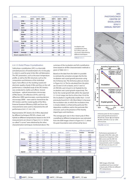
Films Method Incubation Time [min] Crystallisation Time [min]600°C 640°C 680°C 600°C 640°C 680°COTM 300 50 16 780 140 29Raman 360 50 12 720 125 28XRD 270 62 16 1020 120 32UV-R 270 50 14 900 125 32PECVD Average 300 53 14 855 128 30OTM 300 35 11 720 90 23Raman 300 32 10 660 90 24XRD 270 31 12 1020 105 24UV-R 270 31 9 900 90 25E-beam Average 285 32 10 825 94 24OTM 300 45 14 780 130 28Raman 360 40 12 690 120 28XRD 270 60 15 1020 135 30UV-R 270 45 12 900 120 30Hybrid Average 300 48 13 848 126 29Generic equation [4.4.1.19] 660 108 22Incubation andcrystallisation timesfor Si films (solar cellstructures) deposited bydifferent techniques.Table 4.4.1.1ARCPHOTOVOLTAICSCENTRE OFEXCELLENCE2010/11ANNUAL REPORT4.4.1.5 Solid Phase CrystallisationSolid phase crystallisation (SPC) is a thermallyactivated process <strong>of</strong> transformation <strong>of</strong> a-Si into poly-Si, which is used for poly-Si thin-film cell fabrication.The SPC parameters, such as the exact temperaturepr<strong>of</strong>ile, as well as the film structure, such as thecomposition and thickness <strong>of</strong> the individuallayers, have effects on the resulting crystal andelectronic quality <strong>of</strong> poly-Si film and thus on the cellperformance. A detailed study <strong>of</strong> the SPC kineticswas conducted to clarify such effects. Severaltechniques – optical transmission microscopy(OTM), Raman, UV reflection (UV-R), and X-raydiffraction (XRD) spectroscopes, scanning electronmicroscopy (SEM) – were used to characterise theSPC kinetics and the crystal quality <strong>of</strong> the films.External Quantum Efficiency (EQE) and Suns-Vocmeasurements were used to characterise the cellperformance [4.4.1.17, 4.4.1.18].Representative SPC kinetics for Si films depositedby different techniques (PECVD, e-beam, andhybrid) at different temperatures based on the UV-Rmeasurements are shown in Figure 4.4.1.5. Similarso-called “S-curves” were obtained by the othercharacterisation techniques mentioned above. Thesummary <strong>of</strong> the incubation and full crystallisationtimes based on all film characterisation methods isgiven in Table 4.4.1.1.Based on the data from the table it is possibleto estimate the activation energies (Ea) for theincubation and crystal growth processes usingthe Arrhenius law. The Arrhenius plots are shownin Figure 4.4.1.6. The Ea calculated from the plotsare 3.0 and 3.3 eV (e-beam), and 2.7 and 3.2eV (PECVD), and 2.8 and 3.2 eV (hybrid) for theincubation and crystal growth respectively. TheEa for the crystal growth falls within the reported3.1-3.4 eV range, but the Ea <strong>of</strong> less than 3.0 eV forthe incubation is significantly smaller than ~3.4 eVpreviously found [4.4.1.20]. Most likely it is becausethe nucleation rate, to which the incubation timeis closely related, is enhanced by particular filmdeposition conditions and/or the particular filmstructure, such as the presence <strong>of</strong> the heavilydoped layers and interfaces.The average grain size in the e-beam poly-Si filmscrystallised at different temperatures was estimatedfrom the SEM images shown in Figure 4.4.1.7, wherethe grain boundaries were enhanced by Seccoln(1/time) [s -1 ]ln(1/time) [s -1 ]-6-7-8-9-10-7-8-9-10Annealing Temperature [ C]680 640 600IncubationCrystal growth-1112.0 12.5 13.0 13.51/kT [eV -1 ]Arrhenius plots for the incubationand crystal growth processes inPECVD (♦), E-beam (■) and Hybrid(●) films with the n+/p-/p+ solarcell structure.Figure 4.4.1.6E-beam = 3.01 eVHybrid = 2.82 eVPECVD = 2.72 eVE-beam = 3.31 eVHybrid = 3.17 eVPECVD = 3.18 eVFilmsPECVDE-beamHybridV ocJscAbsorber Doping Diffusion Length [nm]T [°C] [mV] [mA/cm 2 ] p.FF [%] p.Eff [%] [/cm 3 ]Emitter Absorber600 474 12.7 76 4.6 5.4×10 15 160 2400640 466 11.5 70 3.8 5.8×10 15 140 1800680 456 10.8 63 3.1 4.6×10 15 135 1500600 474 13.4 76 4.8 9.8×10 15 180 2150640 462 13.3 75 4.6 8.6×10 15 155 2100680 432 12.9 74 4.1 9.5×10 15 120 2000600 459 14.4 75 4.9 2.9×10 15 235 4000600 455 14.1 75 4.8 3.2×10 15 210 4000640 433 13.6 73 4.2 2.5×10 15 170 4000Performance parameters <strong>of</strong>the poly-Si thin film solar cellsobtained by integration <strong>of</strong> theEQE curves over the AM1.5Gsolar spectrum, from Suns-V ocmeasurements, and C-V analysis.All cells have an area <strong>of</strong> 2 cm 2 .Table 4.4.1.2(a)(b)(c)3 m3 m3 mSEM images <strong>of</strong> the fullycrystallized and Secco etchede-beam poly-Si films for differentSPC temperatures.Figure 4.4.1.741


