

Complete Report - University of New South Wales
Complete Report - University of New South Wales
Complete Report - University of New South Wales
- No tags were found...

Create successful ePaper yourself
Turn your PDF publications into a flip-book with our unique Google optimized e-Paper software.
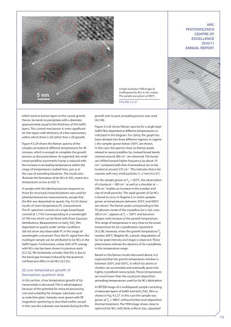
ARCPHOTOVOLTAICSCENTRE OFEXCELLENCE2010/11ANNUAL REPORTA High resolution TEM image <strong>of</strong>multilayered Ge NCs in SiO 2matrix.The sample was grown at 380°C.Figure 4.5.27which work as barrier layers to the crystal growth.Hence, Ge tends to precipitate with a diameterapproximately equal to the thickness <strong>of</strong> the GeROlayers. This control mechanism is more significantfor thin layers with thickness <strong>of</strong> a few nanometers,within which there is 2D rather than a 3D growth.Figure 4.5.24 shows the Raman spectra <strong>of</strong> thesamples annealed at different temperatures for 40minutes, which is enough to complete the growthprocess as discussed above. As expected, the smallnanocrystalline asymmetric hump is reduced withthe increase in annealing temperature within therange <strong>of</strong> temperatures studied here, just as inthe case <strong>of</strong> annealing durations. The results alsoillustrate the formation <strong>of</strong> Ge NCs in SiO 2matrix at atemperature as low as 620 °C.A sample with the identical process sequence asthose for structural characterizations was used forphotoluminescence measurements, except thatthe film was deposited on quartz. Fig. 4.5.25 showsresults <strong>of</strong> room-temperature PL measurement.The PL spectrum consists <strong>of</strong> a single broad bandcentred at 1.77eV (corresponding to a wavelength<strong>of</strong> 700 nm) which can be fitted with three Gaussiandistributions. Measurement on GeO 2/SiO 2filmdeposited on quartz under similar conditionsdid not show any observable PL in the range <strong>of</strong>wavelengths concerned. Thus the PL signal from themultilayer sample can be attributed to Ge NCs in theGeRO layers. Furthermore, a blue shift <strong>of</strong> PL energywith NCs size has been shown in previous work[4.5.32]. We tentatively consider that this is due tothe band gap increase induced by the quantumconfinement effect in Ge NCs [4.5.35].(ii) Low temperature growth <strong>of</strong>Germanium quantum dotsIn this section, a low temperature growth <strong>of</strong> Genanocrystals is discussed. This is advantageousbecause <strong>of</strong> the potential for reduced processingcost and suitability for cheaper substrates suchas soda-lime glass. Samples were grown with RFmagnetron sputtering as described earlier, exceptin this case the substrate was heated during the filmgrowth and no post annealing process was used[4.5.36].Figure 4.5.26 shows Raman spectra for a single layerGeRO film deposited at different temperatures asindicated in the diagram. For clarity, the graph hasbeen divided into three different regimes. In regimeI, the samples grown below 350°C are shown.In this case, the spectra show no Raman peaksrelated to nanocrystalline Ge, instead broad bandscentred around 280 cm -1 are observed. The bandsare shifted toward higher frequency by about 10cm -1 compared with that <strong>of</strong> amorphous Ge (α-Ge)located at around 270 cm -1 . This indicates that α-Gecoexists with very small particles (1~2 nm) [4.5.37].For the sample grown at T g= 320°C, the observation<strong>of</strong> a hump at ~ 280 cm -1 as well as a shoulder at ~298 cm -1 implies an increase in the number andsize <strong>of</strong> small particles. The rapid growth <strong>of</strong> Ge NCsis found to occur in Regime II, in which samplesgrown at temperatures between 350°C and 400°Care shown. The Raman peak corresponding to theTO phonon mode <strong>of</strong> the crystalline Ge (c-Ge), near300.4 cm -1 , appears at T g= 350°C and becomessharper with increase in the growth temperature.This range <strong>of</strong> temperature is very close to the onsettemperature for Ge crystallisation reported in[4.5.38]. However, when the growth temperature T greaches 420°C (Regime III), a drastic degradation <strong>of</strong>Ge-Ge peak intensity and shape is observed. Thesephenomena indicate the absence <strong>of</strong> Ge crystallinityin this temperature range.Based on the Raman results discussed above, it isexpected that the growth temperature window isbetween 350 o C and 420 o C, in which Ge atoms orclusters can accumulate and eventually grow intohighly crystallised nanocrystals. These temperaturesare much lower than the usual post-depositionannealing temperatures used for Ge NCs fabrication.A HRTEM image <strong>of</strong> a multilayered sample consisting<strong>of</strong> alternate layers <strong>of</strong> GeRO and GeO 2/SiO 2films isshown in Fig. 4.5.27. In this case the sample wasgrown at T g= 380 o C without further post-depositionthermal treatment. The TEM image shows close tospherical Ge NCs with fairly uniform size, separated73


