

Complete Report - University of New South Wales
Complete Report - University of New South Wales
Complete Report - University of New South Wales
- No tags were found...

You also want an ePaper? Increase the reach of your titles
YUMPU automatically turns print PDFs into web optimized ePapers that Google loves.
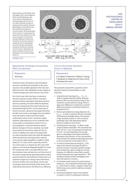
Physical picture <strong>of</strong> the ND HC SolarCell (upper) with a carrier diffusionfield (core/shell thickness rationot to scale), embedded into awide band gap solar cell [4.5.71].Iso-valent impurities provide anenergy selective level for electrons.Band diagram <strong>of</strong> the ND HC SolarCell matched to the physicalstructure (lower). Direct generation<strong>of</strong> hot exciton (1), energy selectiveextraction <strong>of</strong> hot electron from HotCarrier absorber (2), thermionicemission/diffusion <strong>of</strong> holes overthe barrier (3), electron-electronscatteringwith renormalization<strong>of</strong> carrier energies and possibleenergy loss by phonon emission(4), free carrier re-absorption (5),impact ionization (6) and carriergeneration in the wide band gapmatrix (7).ARCPHOTOVOLTAICSCENTRE OFEXCELLENCE2010/11ANNUAL REPORTFigure 4.5.64Nanoparticle cell design incorporatingESCs and absorberResearcher:Dirk KönigA full Hot Carrier cell requires control <strong>of</strong> optical,electronic and phononic properties in the samestructure. One possible approach is the ‘nano-dot(ND) Hot Carrier cell’ embedded into the i-region <strong>of</strong>a wide band gap solar cell as shown in Fig. 4.5.64.Hot Carrier solar cells must have a continuouselectronic density <strong>of</strong> states (DOS) to maximisemaximum photon absorption and elastic electronelectronscattering. The latter refills the depletedelectronic energy levels from which electrons areextracted through the ESC. On the other hand, ifthey do not have a phononic band gap themselvesthe NDs must not be much bigger than the ballisticmean free path in order to prevent inelasticscattering by which carriers cool down rapidly.However, optical phonons can be confined in thenanocrystals as mentioned in Section 4.5.3.3.3by arranging for a mismatch between opticalphonon energies in the two materials. Core shellnanocrystals can be used to realise this [4.5.61,4.5.62]. In addition the shell can be doped withiso-valent impurities which form split-<strong>of</strong>f subbandswithin the electronic band gap <strong>of</strong> the material,such as boron replacing gallium in gallium nitride(GaN) [4.5.71]. Such an ESC would only work forone carrier type as co-doping <strong>of</strong> a thin nano-shellappears not to be technologically feasible. For someIII-V compounds with a very high effective massratio between holes and electrons such that most <strong>of</strong>the excess energy during optical generation is takenup by the electron, thermalisation <strong>of</strong> holes does notrepresent a large loss in energy. Hence thermionicemission <strong>of</strong> holes over a low barrier can be usedto transport holes into the bulk <strong>of</strong> the device to becollected by the junction with little loss in efficiency.4.5.3.3.4 Hot Carrier Absorber:Choice <strong>of</strong> MaterialsResearchers:G. Conibeer, R. Patterson, P. Aliberti, S. Huang,Y. Kamikawa, D. König, Binesh Puthen-Veettil,S.Shrestha, M.A. GreenThe properties required for a good hot carrierabsorber material are listed below in order<strong>of</strong> priority.1. Large phononic band gap (E O(min)- E LA) - inorder to suppress Klemens decay <strong>of</strong> opticalphonons this must be at least as large as themaximum acoustic phonon energy. Hence alarge mass difference (or large force constantdifference) between constituent elements isrequired [4.5.61].2. Narrow optical phonon energy dispersion (E LO-E O(min)) – in order to minimise the loss <strong>of</strong> energyto TO phonons by Ridley decay. This requiresa high symmetry atomic or nano-structure,preferably cubic with degenerate opticalphonon energies at zone centre.3. Small electronic band gap – to allow a widerange <strong>of</strong> photon absorption. This should be lessthan 1eV. For 1 sun concentration the optimumis 0.7eV - as a band gap below this energygives no advantage in the balance betweenabsorption and emission. As the concentrationratio increases this optimum band gap decreasesto zero at maximum concentration [4.5.1].4. A small LO optical phonon energy (E LO). Thisreduces the amount <strong>of</strong> energy lost per LOphonon emission, requiring a greater numberto be emitted for a given energy loss [4.5.62].However, it is difficult to have both a small E LOand the large phononic gap required in 1. Thiscondition requires further investigation, butdoes still argue for a small E LO.5. An absolute small maximum acoustic phononenergy (E LA). This maximises the phononic gap ifE LOis also small. A small E LArequires a large massfor the heavy atom and/or small force constantfor its bonds.6. Good renormalisation rates in the material,i.e. good e-e and h-h scattering (e=electron,91


