

Complete Report - University of New South Wales
Complete Report - University of New South Wales
Complete Report - University of New South Wales
- No tags were found...

Create successful ePaper yourself
Turn your PDF publications into a flip-book with our unique Google optimized e-Paper software.
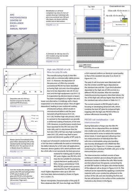
ARCPHOTOVOLTAICSCENTRE OFEXCELLENCE2010/11ANNUAL REPORTMetallisation on cell levelcompleted: top view <strong>of</strong> a 5x5 cm 2sample showing 4 individual cellsplus cross sectional view (SiN andsilica layers not shown) with theemitter and air side busbars.Figure 4.4.1.15A schematic air-side top view <strong>of</strong> amini-module using wire-bondedcell interconnection.Figure 4.4.4.161.210.80.60.40.2Deposition rate <strong>of</strong> a-Si:H as afunction <strong>of</strong> power for the SPCoptimisedPECVD process.Figure 4.4.1.13Raman spectra (normalised) <strong>of</strong> thepoly-Si films obtained by SPC <strong>of</strong> thestandard (pink) and high (blue) ratePECVD a-Si:H. The spectrum <strong>of</strong> c-Siis (black) shown for reference.Figure 4.4.1.14Absorber deposition rate,nm/minSuns-Voc results (the average <strong>of</strong> fivepoints) after RTA and hydrogenation<strong>of</strong> SPC poly-Si diodes on AITglass with PECVD a-Si:H absorberdeposited at 35 nm/min (“low rate”)250 nm/min (“high rate”).Table 4.4.1.71-Sun Voc,mVhi gh r at estd. rateS i wa f e r0505 510 515 520 525 530 535n=1 Voc,mVHigh rate PECVD <strong>of</strong> a-Sifilms for poly-Si cellsThe manufacturing <strong>of</strong> poly-Si thin-filmsolar cells is a commercially viable process[4.4.1.1]. However, the deposition <strong>of</strong>the precursor a-Si films by currentlyconventional PECVD has been identifiedas having high cost and a low throughputdue to its low deposition rate (25-35 nm/min) and the high equipment cost [4.4.1.3].Si evaporation by electron beam (e-beam)has been investigated as a higher rate andlower cost alternative. A challenge with e-beamevaporation is its directional nature (“line-<strong>of</strong>-sight”deposition), leading to non-conformal coating<strong>of</strong> textured surfaces, which results inmicrostructural defects and the poortextured cell performance [4.4.1.25,4.4.1.26]. Another high rate process, whichin contrast to the evaporation can providea conformal coating <strong>of</strong> textures, is hot-wireCVD. However, no performance results havebeen reported for the SPC hot-wire CVDsolar cells, and it is also known that thehot-wire CVD a-SiH has very high nucleationrates [4.4.1.23], which may lead to poorcrystal and electronic quality <strong>of</strong> SPC poly-Si.A major part <strong>of</strong> research conducted on PECVD <strong>of</strong>a-Si:H has been traditionally focused on minimisingthe defect density for a-Si:H solar cell applications.However, device-grade a-Si:H, which performs wellfor a-Si:H cells, is not necessarily the best precursormaterial for making poly-Si cells byn=2 Voc,mV35 494.6 ± 8.9 496 666250 512.4 ± 4.5 513 711SPC and a higher rate PECVD a-Si:Hmay also be suitable for producinga good electronic quality poly-Sifilms. Using a conventional 13.56MHz PECVD system and a processoptimised for the SPC application,much higher deposition rates up to 265 nm/min have been demonstrated as shown in Figure4.4.1.13 [4.4.1.7].Raman microprobe characterisation <strong>of</strong> the poly-Sifilms obtained after SPC from the high rate PECVDa-Si:H material confirms an identical crystal qualityto that <strong>of</strong> the standard rate poly-Si as shown inFigure 4.4.1.14.The poly-Si cell structures were fabricated withthe thin emitter and BSF layers deposited atthe standard rate and the ~2 µm thick absorberdeposited at the high rate <strong>of</strong> 250 nm/min in adifferent PECVD chamber. After the standardmaterial processing sequence described above, theVoc <strong>of</strong> the high rate cell was higher than the Voc <strong>of</strong>the standard rate cell as shown in Table 4.4.1.7.The current research in PECVD poly-Si cells isfocusing on developing advanced cells, whichcombine the best AIT glass for enhanced lighttrapping with the high rate PECVD Si films toachieve efficiencies exceeding 10%.PECVD cell metallisation – cellinterconnectionDuring fabrication <strong>of</strong> large size thin-film PVmodules, the as-deposited films are dividedinto smaller area unit cells, which are theninterconnected in series to reduce the resistiveohmic losses. A novel approach allowing a lowloss interconnection <strong>of</strong> individual thin-filmcells into a minimodule using wire-bondingwas recently developed in the UNSW thin filmgroup [4.4.1.9]. Figure 4.4.1.15 shows a samplecontaining four individual PLASMA cells prior to theinterconnection process.The interconnection method consists <strong>of</strong> laserscribing an isolation groove along the glass sidealuminium busbar to define the cells. Wire-bondsare then placed over this groove, connecting theair-side BSF busbar to the glass side emitter busbar<strong>of</strong> the adjacent cell as shown in Figure 4.4.4.16. Thismethod can be expanded by applying a conductivematerial (with a non-conductive adhesive) to thesurface <strong>of</strong> the cell, and wire-bonding the first andthe last cell busbars to the surface <strong>of</strong> the conductivematerial as also shown in the figure.44


