

Complete Report - University of New South Wales
Complete Report - University of New South Wales
Complete Report - University of New South Wales
- No tags were found...

Create successful ePaper yourself
Turn your PDF publications into a flip-book with our unique Google optimized e-Paper software.
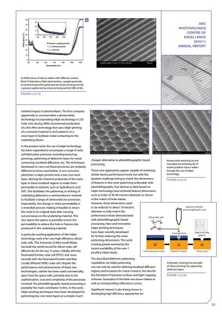
Reflectance (%)8070605040302025201510400 550 700 850 1000Random upright pyramidsI.J. inverted pyramidsI.J. v-groovesARCPHOTOVOLTAICSCENTRE OFEXCELLENCE2010/11ANNUAL REPORT100300 450 600 750 900 1050 1200Wavelength (nm)(a) Reflectance <strong>of</strong> silicon wafers with different surfacefinish (i) laboratory fabricated random, upright pyramids,(ii) inverted pyramids patterned by ink jet printing and (iii)v-grooves patterned by ink jet printing and (b) SEM <strong>of</strong> (iii).Figure 4.3.2.18minimal impact in photovoltaics. The first companyapparently to commercialise a photovoltaictechnology incorporating inkjet technology is CSGSolar who during 2006 commenced production<strong>of</strong> a thin-film technology that uses inkjet printing<strong>of</strong> a corrosive material to etch patterns in aresist layer to facilitate metal contacting to theunderlying silicon.In the present work, the use <strong>of</strong> inkjet technologyhas been expanded to encompass a range <strong>of</strong> solarcell fabrication processes including texturing,grooving, patterning <strong>of</strong> dielectric layers for metalcontacting, localized diffusions, etc. The techniquesdeveloped to carry out these processes are uniquelydifferent to those used before. A non-corrosiveplasticizer is inkjet printed onto a low cost resistlayer, altering the chemical properties <strong>of</strong> the resistlayer in these localized regions to make thempermeable to etchants such as hydr<strong>of</strong>luoric acid(HF). This facilitates the patterning or etching <strong>of</strong>underlying dielectrics or semiconductor materialto facilitate a range <strong>of</strong> semiconductor processes.Importantly, the change in resist permeability isa reversible process making it feasible to returnthe resist to its original state after carryingout processes on the underlying material. Thisalso opens the option to partially reverse thepermeability to reduce the hole or feature sizeproduced in the underlying material.A particular exciting application <strong>of</strong> this inkjettechnology work is for very high efficiency siliconsolar cells. The <strong>University</strong> <strong>of</strong> <strong>New</strong> <strong>South</strong> <strong>Wales</strong>has held the world record for silicon solar cellefficiencies for the last 15 years, initially with thePassivated Emitter solar cell (PESC) and morerecently with the Passivated Emitter and RearLocally diffused (PERL) solar cell. Despite theperformance and achievements <strong>of</strong> these twotechnologies, neither has been used commercially,apart from for space cells, primarily due to thesophistication, cost and complexity <strong>of</strong> the processesinvolved. The photolithographic based processing isprobably the main contributor to this. In this work,inkjet printing techniques have been developed forpatterning low cost resist layers as a simple, muchcheaper alternative to photolithographic basedprocessing.These new approaches appear capable <strong>of</strong> achievingsimilar device performance levels but with thegreatest challenge being to match the dimensions<strong>of</strong> features in the resist patterning achievable withphotolithography. Test devices to date based oninkjet technology have achieved feature dimensionssuch as holes <strong>of</strong> 30-40 microns diameter as shownin the matrix <strong>of</strong> holes below.However, these dimensions needto be reduced to about 10 micronsdiameter to fully match theperformance levels demonstratedwith photolithographic basedprocessing. <strong>New</strong> and innovativeinkjet printing techniqueshave been recently developedfor further reducing the resistpatterning dimensions. This workis being greatly assisted by therecent availability <strong>of</strong> the new 1picolitre inkjet heads.The described dielectric patterningcapabilities via inkjet patterningcan not only be used for defining localized diffusionregions and locations for metal contacts, but also forthe formation if textured surfaces and light trappingschemes. Examples <strong>of</strong> the latter are shown below aswell as corresponding reflectance curves.Significant interest is also being shown indeveloping high efficiency approaches forHoneycomb texturing (a) andmacrogroove texturing (b) <strong>of</strong>multicrystalline silicon wafersthrough the use <strong>of</strong> inkjettechnology.Figure 4.3.2.19Schematic showing the principle<strong>of</strong> “Direct Etching” for patterningdielectric layers.Figure 4.3.2.2033


