

Complete Report - University of New South Wales
Complete Report - University of New South Wales
Complete Report - University of New South Wales
- No tags were found...

You also want an ePaper? Increase the reach of your titles
YUMPU automatically turns print PDFs into web optimized ePapers that Google loves.
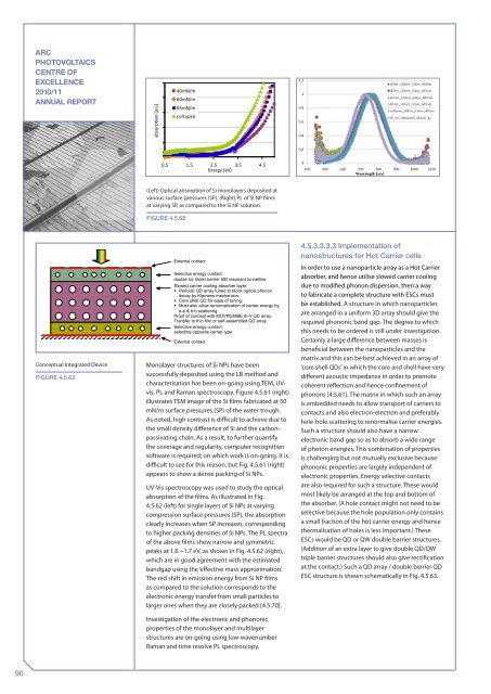
ARCPHOTOVOLTAICSCENTRE OFEXCELLENCE2010/11ANNUAL REPORTabsorption (a.u)40mN/m60mN/m65mN/mcollapse0.5 1.5 2.5 3.5 4.5Energy (eV)(Left) Optical absorption <strong>of</strong> Si monolayers deposited atvarious surface pressures (SP). (Right) PL <strong>of</strong> Si NP filmsat varying SP, as compared to the Si NP solution.Figure 4.5.62Conceptual Integrated DeviceFigure 4.5.63External contactSelective energy contact:double (or triple) barrier QD resonant tunnellingSlowed carrier cooling absorber layer:§ Periodic QD array tuned to block optical phonondecay by Klemens mechanism;§ Core shell QD for ease <strong>of</strong> tuning;§ Must also allow renormalization <strong>of</strong> carrier energy bye-e & h-h scattering.Pro<strong>of</strong> <strong>of</strong> concept with MOVPE/MBE III-V QD array.Transfer to thin film or self-assembled QD array.Selective energy contact:selecting opposite carrier typeExternal contactMonolayer structures <strong>of</strong> Si NPs have beensuccessfully deposited using the LB method andcharacterisation has been on-going using TEM, UVvis,PL and Raman spectroscopy. Figure 4.5.61 (right)illustrates TEM image <strong>of</strong> the Si films fabricated at 50mN/m surface pressures (SP) <strong>of</strong> the water trough.As noted, high contrast is difficult to achieve due tothe small density difference <strong>of</strong> Si and the carbonpassivatingchain. As a result, to further quantifythe coverage and regularity, computer recognitions<strong>of</strong>tware is required; on which work is on-going. It isdifficult to see for this reason, but Fig. 4.5.61 (right)appears to show a dense packing <strong>of</strong> Si NPs.UV-Vis spectroscopy was used to study the opticalabsorption <strong>of</strong> the films. As illustrated in Fig.4.5.62 (left) for single layers <strong>of</strong> Si NPs at varyingcompression surface pressures (SP), the absorptionclearly increases when SP increases, correspondingto higher packing densities <strong>of</strong> Si NPs. The PL spectra<strong>of</strong> the above films show narrow and symmetricpeaks at 1.6 ~1.7 eV, as shown in Fig. 4.5.62 (right),which are in good agreement with the estimatedbandgap using the ‘effective mass approximation’.The red shift in emission energy from Si NP filmsas compared to the solution corresponds to theelectronic energy transfer from small particles tolarger ones when they are closely packed [4.5.70].Investigation <strong>of</strong> the electronic and phononicproperties <strong>of</strong> the monolayer and multilayerstructures are on-going using low-wavenumberRaman and time resolve PL spectroscopy.4.5.3.3.3.3 Implementation <strong>of</strong>nanostructures for Hot Carrier cellsIn order to use a nanoparticle array as a Hot Carrierabsorber, and hence utilise slowed carrier coolingdue to modified phonon dispersion, then a wayto fabricate a complete structure with ESCs mustbe established. A structure in which nanoparticlesare arranged in a uniform 3D array should give therequired phononic band gap. The degree to whichthis needs to be ordered is still under investigation.Certainly a large difference between masses isbeneficial between the nanoparticles and thematrix and this can be best achieved in an array <strong>of</strong>‘core shell QDs’ in which the core and shell have verydifferent acoustic impedance in order to promotecoherent reflection and hence confinement <strong>of</strong>phonons [4.5.61]. The matrix in which such an arrayis embedded needs to allow transport <strong>of</strong> carriers tocontacts and also electron-electron and preferablyhole-hole scattering to renormalise carrier energies.Such a structure should also have a narrowelectronic band gap so as to absorb a wide range<strong>of</strong> photon energies. This combination <strong>of</strong> propertiesis challenging but not mutually exclusive becausephononic properties are largely independent <strong>of</strong>electronic properties. Energy selective contactsare also required for such a structure. These wouldmost likely be arranged at the top and bottom <strong>of</strong>the absorber. (A hole contact might not need to beselective because the hole population only containsa small fraction <strong>of</strong> the hot carrier energy and hencethermalisation <strong>of</strong> holes is less important.) TheseESCs would be QD or QW double barrier structures.(Addition <strong>of</strong> an extra layer to give double QD/QWtriple barrier structures should also give rectificationat the contact.) Such a QD array / double barrier QDESC structure is shown schematically in Fig. 4.5.63.90


