

Complete Report - University of New South Wales
Complete Report - University of New South Wales
Complete Report - University of New South Wales
- No tags were found...

Create successful ePaper yourself
Turn your PDF publications into a flip-book with our unique Google optimized e-Paper software.
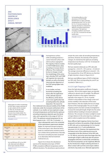
ARCPHOTOVOLTAICSCENTRE OFEXCELLENCE2010/11ANNUAL REPORT(a) Annealing effects on theabsorbance <strong>of</strong> P3HT/PCBMblended layers on glass substrate(temperatures from 125°C to 145°Cfor 5 to 15 minutes duration). (b)Average absorbance compared fordifferent annealing temperaturesand duration. The optimumannealing conditions were foundas 125°C for 15 minutes for the bestquality layer.Figure 4.4.2.4AFM images <strong>of</strong> surface morphology<strong>of</strong> P3HT layer on glass substrate (a)as spin coated; and (b) annealedat 140°C for 10 minutes. Afterannealing the layer structurebecome more clearly visible. Thesurface roughness is also reducedby annealing.Figure 4.4.2.3Voc and fill-factor (FF) <strong>of</strong> our OPVcells, fabricated with differentdonor type materials <strong>of</strong> P3HT.Table 4.4.2.1homogeneous surface,while annealing produces acoarser textured surface withobvious phase segregation.The majority <strong>of</strong> device studieson P3HT:PCBM blends utilizeannealing to increase deviceefficiency. This is believed tobe due to changes in boththe morphology <strong>of</strong> the activelayer whereby P3HT and PCBMself-organize into nanoscaledomains as well as the betterintermolecular alignment <strong>of</strong>the P3HT giving higher holemobilities.In our studies, we havefound that annealing thedevice after the application<strong>of</strong> the cathode improvesthe efficiency <strong>of</strong> the devicemuch more significantly thatannealing before the cathodedeposition. The reason forthis is believed to be reduced mobility <strong>of</strong> the PCBMmolecules under the increased confinement <strong>of</strong> thecathode. In our studies we have explored a range<strong>of</strong> anneal temperatures and find that the optimumannealing temperature depends upon the blendratio, and in general lies in the range <strong>of</strong> 120°C to150°C. The optimum anneal temperature for ourblend appears to be ~125°C (for 15 minutes) – avalue subsequently used in the remainder<strong>of</strong> the optimization experiments detailedbelow. An improved transport property<strong>of</strong> the active layer is also observed whichleads to a reduced series resistance and inturn a better device performance. Recently,microwave annealing has been proposedas an alternative thermal treatmentmethod [4.4.2.5].Figure 4.4.2.4 shows the absorbancespectra <strong>of</strong> the blended active layer <strong>of</strong> P3HT/PCBM, annealed at different temperature and fordifferent durations. The absorbance spectra almostremain the same under all annealing temperaturesand times. However, the intensity <strong>of</strong> the spectrachanges. As mentioned, the optimum annealingtemperature was found as 125°C for 15 minutes forthe best quality layer.We have started to fabricate our OPV cells withaverage Voc ≈ 0.6 V, FF ≈ 70 % and Jsc ≈ 10 mA/cm 2 .The average conversion efficiency is around 3 - 4%.The measured Voc <strong>of</strong> our OPV devices as a function<strong>of</strong> light intensity is shown in Figure 4.4.2.5.We have used different types <strong>of</strong> P3HT to fabricateour OPV cells. Their corresponding Voc and FF arerecorded in Table 4.4.2.1.4.4.2.5 Light Trapping in OPVGiven the high absorption coefficient <strong>of</strong> organicmaterials, 100 nm thick organic layers are typicallysufficient to absorb most <strong>of</strong> sunlight. The diffusionlength <strong>of</strong> excitons in the organic materials istypically in the range <strong>of</strong> 5–10 nm. A partialsolution to the problem <strong>of</strong> low charge carrier andexciton mobility is the reduction <strong>of</strong> the activelayer thickness, that also implies the loss <strong>of</strong> a largefraction <strong>of</strong> the impinging light. The use <strong>of</strong> a lighttrapping systems has been actively investigated toincrease the total path length <strong>of</strong> light into the activematerial without needing to increase its physicalthickness. The concept is to induce sunlight to travela longer distance in the active layer by a multi-passpath in order to exploit most <strong>of</strong> the radiation.Many different light trapping schemes have beenproposed to enhance the quantity <strong>of</strong> light absorbedin OPV cells such as metal gratings [4.4.2.6], buriednanoelectrodes [4.4.2.7] and multireflectionstructures [4.4.2.8]. However, the requirement thatthe feature sizes <strong>of</strong> the scattering structures becomparable to the film thickness <strong>of</strong> the OPV cells,i.e., 50–300 nm, and at the same time larger than thewavelength <strong>of</strong> light to effectively alter the photonpropagation direction is intrinsically contradictory.The electrical properties can be negatively affectedby the introduction <strong>of</strong> light scattering elements indirect contact with such thin active layers: defectsand shorts may easily occur. Alternate approaches56


