

Complete Report - University of New South Wales
Complete Report - University of New South Wales
Complete Report - University of New South Wales
- No tags were found...

You also want an ePaper? Increase the reach of your titles
YUMPU automatically turns print PDFs into web optimized ePapers that Google loves.
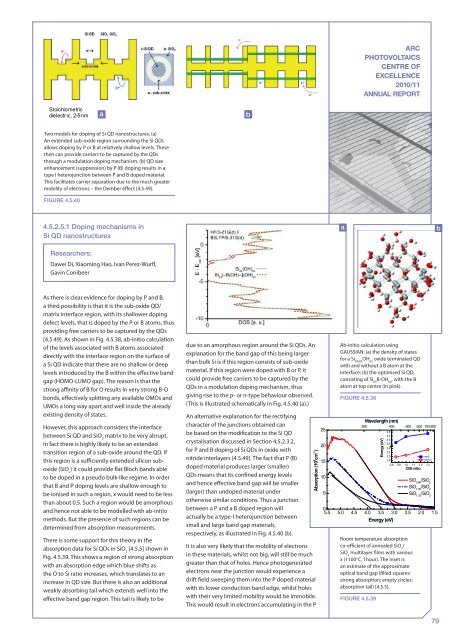
ARCPHOTOVOLTAICSCENTRE OFEXCELLENCE2010/11ANNUAL REPORTStoichiometricdielectric, 2-5nm a) b)Two models for doping <strong>of</strong> Si QD nanostructures. (a)An extended sub-oxide region surrounding the Si QDsallows doping by P or B at relatively shallow levels. Thesethen can provide carriers to be captured by the QDsthrough a modulation doping mechanism. (b) QD sizeenhancement (suppression) by P (B) doping results in atype I heterojunction between P and B doped material.This facilitates carrier separation due to the much greatermobility <strong>of</strong> electrons – the Dember effect [4.5.49].Figure 4.5.404.5.2.5.1 Doping mechanisms inSi QD nanostructuresResearchers:Dawei Di, Xiaoming Hao, Ivan Perez‐Wurfl,Gavin ConibeerAs there is clear evidence for doping by P and B,a third possibility is that it is the sub-oxide QD/matrix interface region, with its shallower dopingdefect levels, that is doped by the P or B atoms, thusproviding free carriers to be captured by the QDs[4.5.49]. As shown in Fig. 4.5.38, ab-initio calculation<strong>of</strong> the levels associated with B atoms associateddirectly with the interface region on the surface <strong>of</strong>a Si QD indicate that there are no shallow or deeplevels introduced by the B within the effective bandgap (HOMO-LUMO gap). The reason is that thestrong affinity <strong>of</strong> B for O results in very strong B-Obonds, effectively splitting any available OMOs andUMOs a long way apart and well inside the alreadyexisting density <strong>of</strong> states.However, this approach considers the interfacebetween Si QD and SiO 2matrix to be very abrupt.In fact there is highly likely to be an extendedtransition region <strong>of</strong> a sub-oxide around the QD. Ifthis region is a sufficiently extended silicon suboxide(SiO x) it could provide flat Bloch bands ableto be doped in a pseudo bulk-like regime. In orderthat B and P doping levels are shallow enough tobe ionised in such a region, x would need to be lessthan about 0.5. Such a region would be amorphousand hence not able to be modelled with ab-initiomethods. But the presence <strong>of</strong> such regions can bedetermined from absorption measurements.There is some support for this theory in theabsorption data for Si QDs in SiO 2[4.5.5] shown inFig. 4.5.39. This shows a region <strong>of</strong> strong absorptionwith an absorption edge which blue shifts asthe O to Si ratio increases, which translates to anincrease in QD size. But there is also an additionalweakly absorbing tail which extends well into theeffective band gap region. This tail is likely to bedue to an amorphous region around the Si QDs. Anexplanation for the band gap <strong>of</strong> this being largerthan bulk Si is if this region consists <strong>of</strong> sub-oxidematerial. If this region were doped with B or P, itcould provide free carriers to be captured by theQDs in a modulation doping mechanism, thusgiving rise to the p- or n-type behaviour observed.(This is illustrated schematically in Fig. 4.5.40 (a).)An alternative explanation for the rectifyingcharacter <strong>of</strong> the junctions obtained canbe based on the modification to the Si QDcrystalisation discussed in Section 4.5.2.3.2,for P and B doping <strong>of</strong> Si QDs in oxide withnitride interlayers [4.5.49]. The fact that P (B)doped material produces larger (smaller)QDs means that its confined energy levelsand hence effective band gap will be smaller(larger) than undoped material underotherwise similar conditions. Thus a junctionbetween a P and a B doped region willactually be a type-I heterojunction betweensmall and large band gap materials,respectively, as illustrated in Fig. 4.5.40 (b).It is also very likely that the mobility <strong>of</strong> electronsin these materials, whilst not big, will still be muchgreater than that <strong>of</strong> holes. Hence photogeneratedelectrons near the junction would experience adrift field sweeping them into the P doped materialwith its lower conduction band edge, whilst holeswith their very limited mobility would be immobile.This would result in electrons accumulating in the PAbsorption (10 6 cm -1 )252015105Ab-initio calculation usingGAUSSIAN: (a) the density <strong>of</strong> statesfor a Si 83/84OH 62oxide terminated QDwith and without a B atom at theinterface; (b) the optimised Si QD,consisting <strong>of</strong> Si 83B-OH 62, with the Batom at top centre (in pink).Figure 4.5.3805.5 5.0 4.5 4.0 3.5 3.0 2.5 2.0 1.5Energy (eV)Room temperature absorptionco-efficient <strong>of</strong> annealed SiO x/SiO 2multilayer films with variousx (1100 o C, 1hour). The inset isan estimate <strong>of</strong> the approximateoptical band gap (filled squares:strong absorption; empty circles:absorption tail) [4.5.5].Figure 4.5.39Wavelength (nm)300 400 500 600 700 800Energy (eV)4.84.44.03.62.42.22.01.8m=2m=1/20.8 0.9 1.0 1.1 1.2 1.3O/Si ratioSiO 0.86/SiO 2SiO 1.00/SiO 2SiO 1.30/SiO 279


